Chapter 6
Differential and Multistage Amplifiers
Gordon W. Roberts
Department of Electrical & Computer Engineering, McGill University
Up to this point we have mainly been looking at transistor circuits driven by unbalanced inputs (i.e., one terminal of the signal source is grounded). A more important transistor arrangement is one that receives differential or balanced input signals. The differential pair is one such example and is used extensively in present day monolithic IC operational amplifiers. In this chapter we shall demonstrate how one generates the appropriate input signals for investigating the behavior of differential amplifiers. Following this, we shall investigate several circuits involving differential and multistage amplifiers. This will also include an investigation of various types of current mirrors and current sources.
|
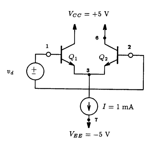
Fig. 6.1: A BJT differential pair driven by a differential input signal without a defined input common-mode level. Driving a differential amplifier in this way is not recommended.
|
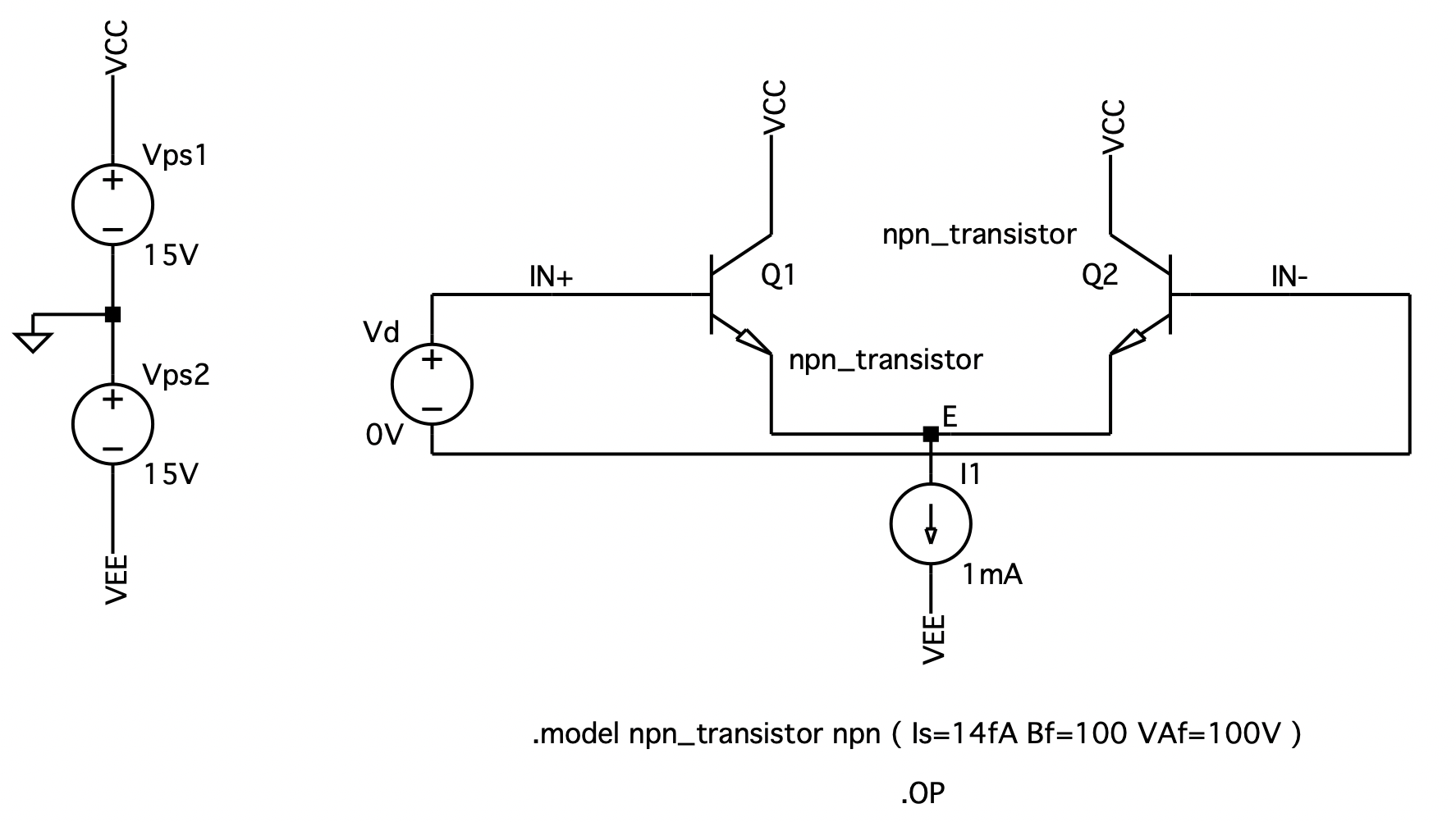
Fig. 6.2: Schematic circuit captured by LTSpice with Spice directives. |
6.1 Input Excitation for the Differential Pair
The differential pair, shown in Fig. 6.1, is the most widely used circuit building block in analog integrated circuits. Its operation is based on the fact that only the difference between the signals appearing at the two inputs is amplified. The signals appearing as common mode at the amplifier inputs are (ideally) not amplified. In the following we would like to use LTSpice to investigate the effect of varying the input common-mode and differential-mode signal levels on the collector currents. The focus of this problem is not so much on the behavior of the differential pair, but rather on how we generate the input signals for differential amplifiers within LTSpice.
For example, to analyze the behavior of a differential pair subject to a differential input signal, first-time users of LTSpice are often tempted to apply a single ungrounded source to the amplifier input as illustrated in Fig. 6.1. Unfortunately, due to the lack of a defined common-mode input level, erroneous data is generated by LTSpice. To see this, we perform a DC analysis of the differential pair captured by LTSpice shown in Fig. 6.2 assuming the BJTs had the following parameters: IS=14 fA, βF=100 and VAF=100 V.
The results of the DC analysis are then found in the Spice Error Log file as follows:
|
Operating Bias Point Solution:
V(vcc) 15 voltage V(in+) -22295.5 voltage V(e) -22296 voltage V(vee) -15 voltage V(in-) -22295.5 voltage
Ic(Q2) 0.0005 device_current Ib(Q2) 5.02026e-19 device_current Ie(Q2) -0.0005 device_current Ic(Q1) 0.0005 device_current Ib(Q1) 5.02026e-19 device_current Ie(Q1) -0.0005 device_current I(I1) 0.001 device_current I(Vd) -3.46945e-18 device_current I(Vps2) -0.001 device_current I(Vps1) -0.001 device_current
|
As is evident from these results, we see that the DC voltage appearing at the two inputs to the differential pair (nodes IN+ and IN-), and at the emitters of the two transistors (node E), are very large negative levels, outside the limits of the supply voltages. Certainly, these levels would not be observed in any real circuit. The reason for this, as just mentioned, is the lack of a common-mode input level and can be corrected by revising the input excitation to include a common-mode level amongst the differential component.
|
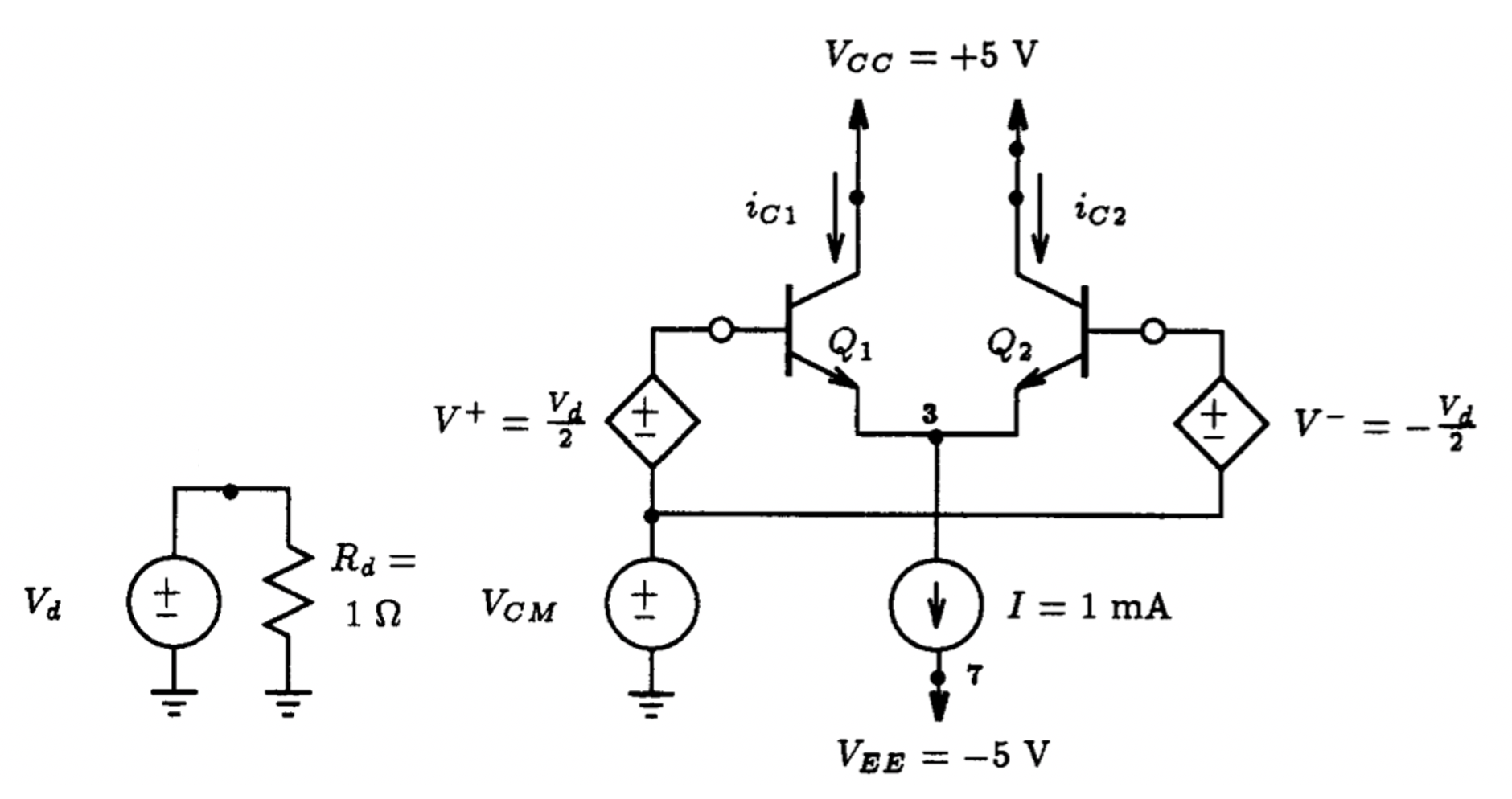
Fig. 6.3: A BJT differential pair driven by a set of input voltage sources arranged such that the common-mode and differential voltage components can be independently varied. But, more importantly, both components will always exist, and are clearly defined. Voltage sources Vic1 and Vic2 are used to monitor the collector current of each transistor.
|
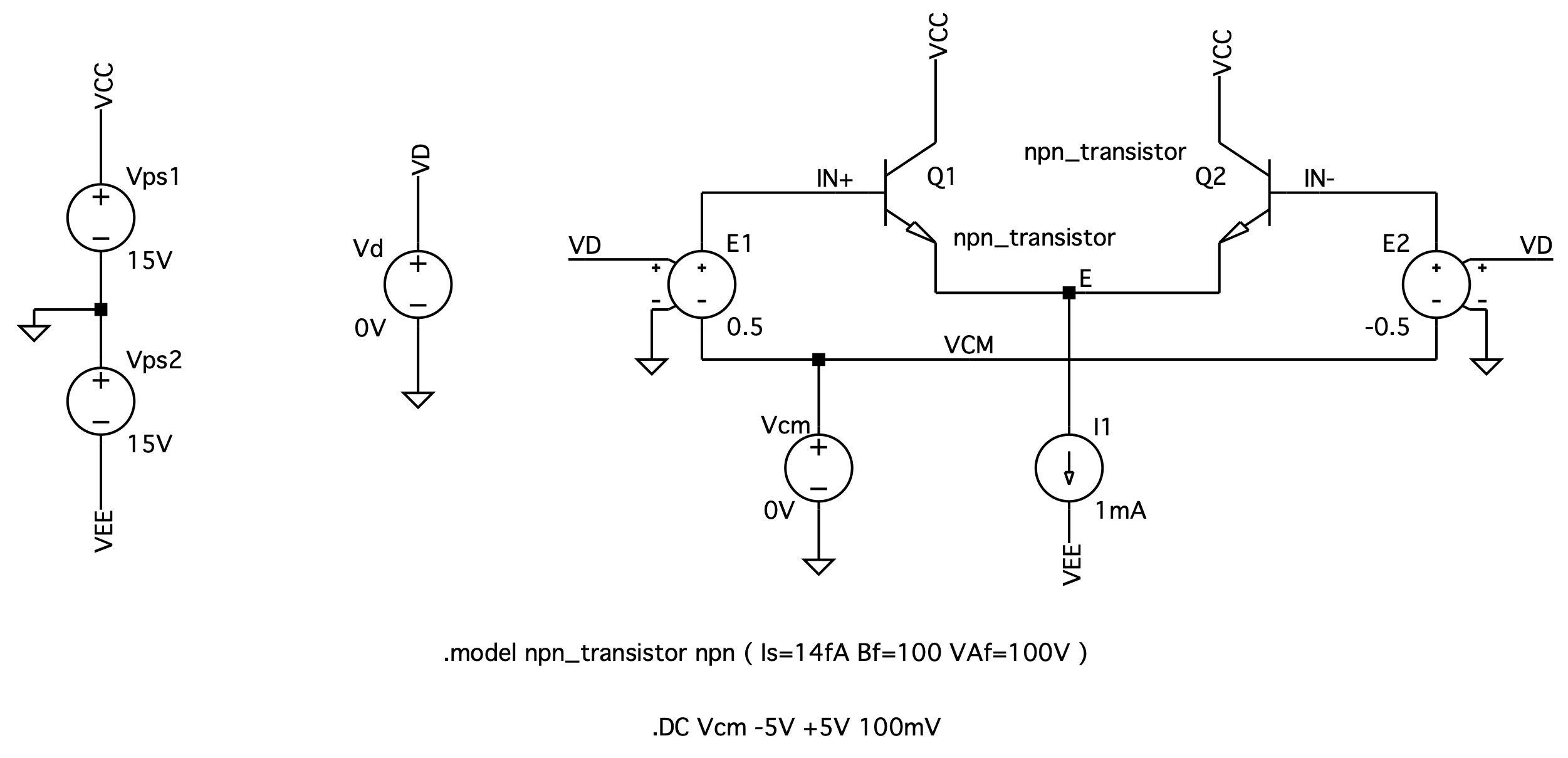
Fig. 6.4: The schematic captured by LTSpice. |
|
Fig. 6.5: The collector currents of the BJT differential pair for a range of input common-mode levels.
|
Fig. 6.6: The collector currents of the BJT differential pair versus the level of differential input signal.
|
The circuit shown in Fig. 6.3 accomplishes this in a convenient way. It allows the input common-mode level to be adjusted by varying the value of VCM, independent of the value of the differential-mode component being established by the two VCVSs connected across the input terminals of the differential pair. The level of each VCVS is one-half the voltage value set by the isolated voltage source Vd. This voltage source is loaded arbitrarily in a 1Ω resistor in order to satisfy the Spice requirement that every node in a circuit has at least two connections.
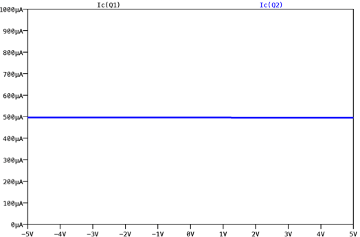
To demonstrate the versatility of this input-source arrangement, we shall investigate the effect of separately varying the input common-mode and differential signal components on the collector currents of the differential pair of Fig. 6.3. The LTSpice schematic captured file describing this circuit is displayed in Fig. 6.4. The parameters of the npn BJTs are assumed to be the same as before (i.e., IS=14 fA, βF=100 and VAF=100 V). As our first analysis request, we are asking that LTSpice perform a DC sweep of the input common-mode voltage level VCM beginning at -5 V and ending at +5 V in increments of 100 mV. The differential input component Vd is set to zero during this analysis, thus also making IN+ and IN- equal to VCM. On completion of LTSpice we observe in Fig. 6.5 the behavior of the two collector currents as a function of VCM. Here we see that both Q1 and Q2 are conducting equal currents of 0.5 mA for all input common-mode levels.
To investigate the effect of a differential signal appearing at the input terminals of the differential pair, we simply revise the Spice directive given in Fig. 6.4 and replace the DC sweep command given there by the following one:
.DC Vd -500mV +500mV 10mV
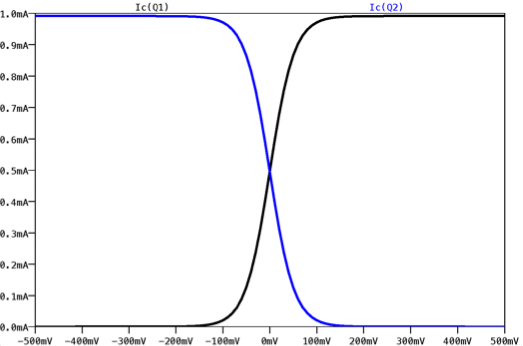
Here we are requesting that LTSpice vary the level of Vd between -500 mV and +500 mV in 10 mV increments. The common-mode input level VCM is to remain at 0 V throughout this analysis. On completion of the LTSpice analysis, the collector currents displayed in Fig. 6.6 are found. Here the results are as expected: Depending on the level of input differential signal, the biasing current of 1 mA is steered between the two transistors.
|
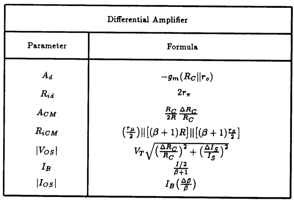
Table 6.1: General expressions for estimating the small-signal behavior of the differential amplifier shown in Fig. 6.7. Note that R is the output resistance of the current source I.
|
|
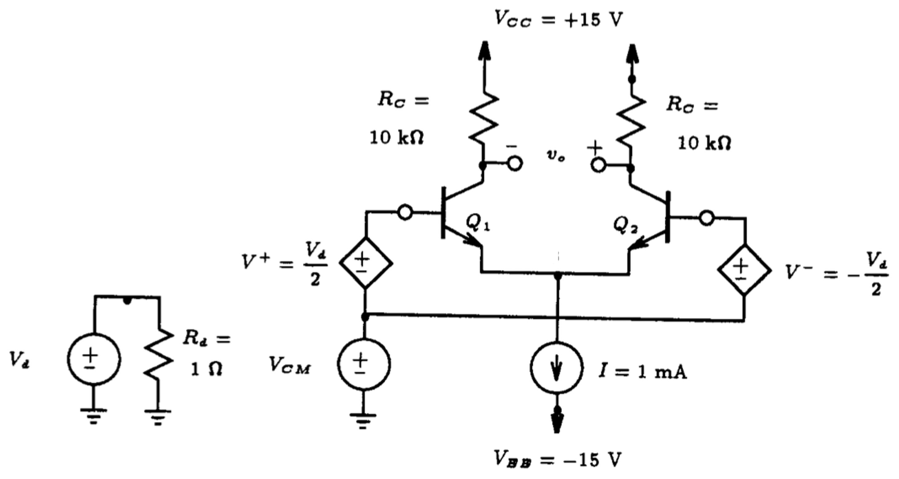
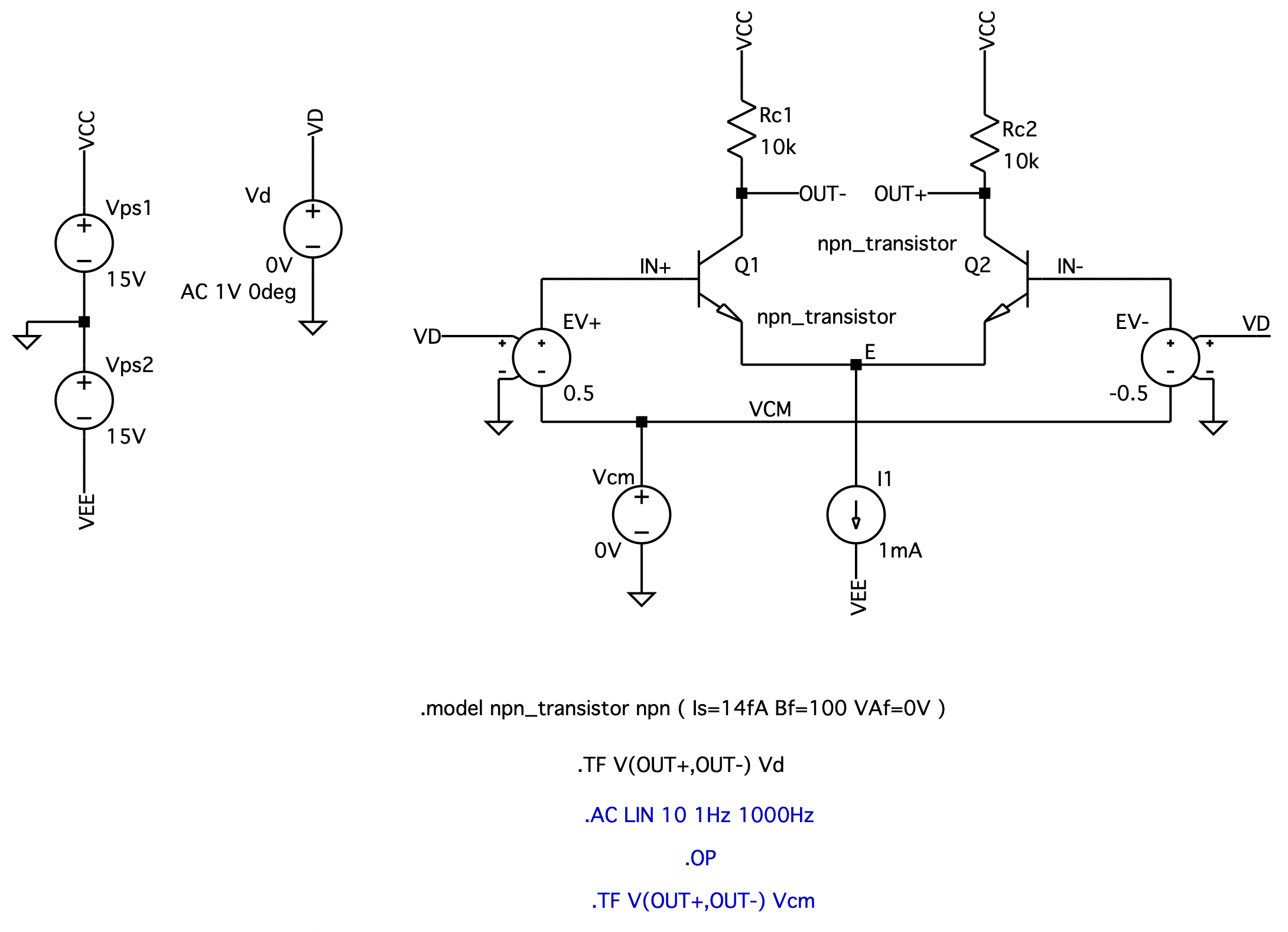
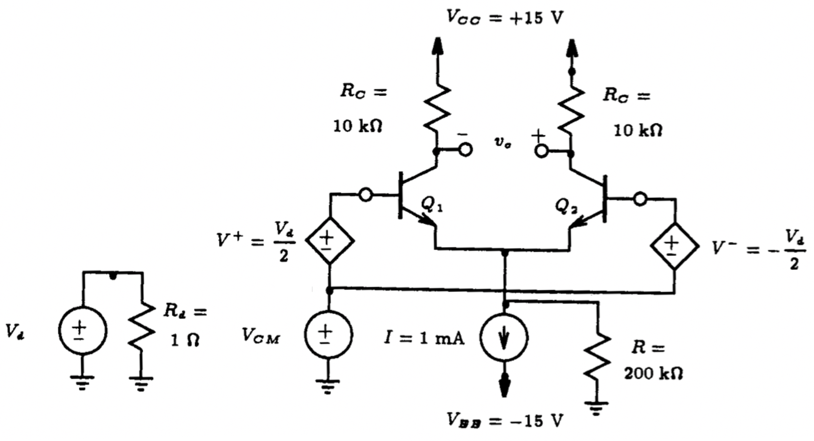
Fig. 6.7: The basic BJT differential-pair amplifier configuration driven with the multiple-input source arrangement described in Section 6.1.
|
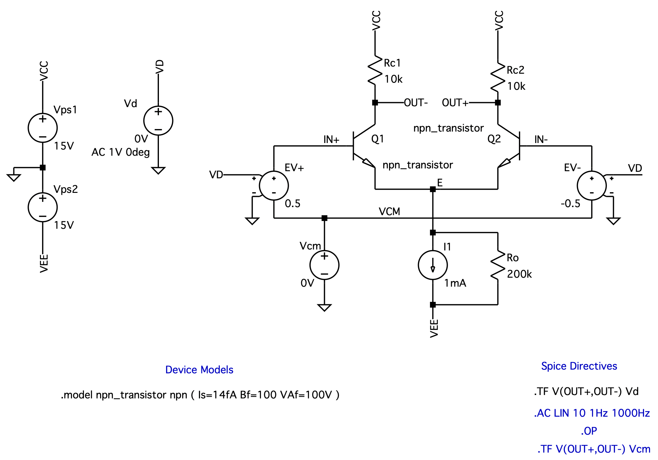
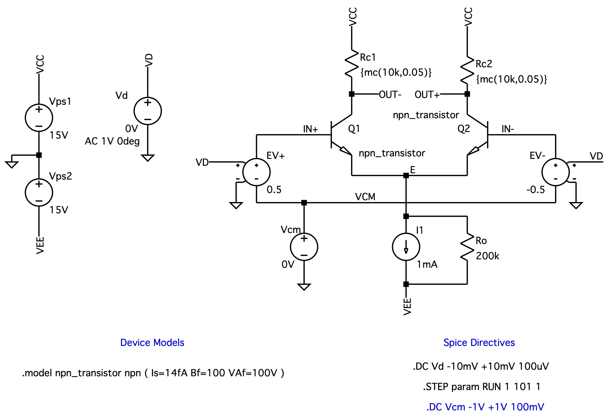
Fig. 6.8: The schematic captured by LTSpice for calculating the 2-port equivalent of the differential amplifier shown in Fig. 6.7. Several Spice directives are used in this example.
|
6.2 Small-Signal Analysis of the Differential Amplifier: Symmetric Conditions
In this section we investigate the small-signal behavior of the BJT differential-pair amplifier configuration shown in Fig. 6.7 using LTSpice. We shall assume throughout this section that the circuit remains symmetric, i.e., the resistances in collectors are equal and transistors Q1 and Q2 are matched. Our purpose here is twofold: to illustrate how one uses LTSpice to determine the small-signal behavior of a differential amplifier, such as that shown in Fig. 6.7, using the multiple-input source arrangement discussed in the previous section, and to determine the accuracy of the expressions that are derived by hand analysis.
It is important to point out that when one compares results computed by LTSpice to those computed through the application of closed-form expressions derived by hand analysis from a small-signal circuit model of the transistor circuit, the accuracy of the results depend on two factors: (1) how precise the estimate of the values of the parameters of the small-signal model is, and (2) how accurate the small-signal expressions are; given that certain simplifying assumptions are made in their development. Within this section, we are simply addressing the second issue; that being, the accuracy of the expressions derived by hand for the BJT differential amplifier under various circuit conditions. This is accomplished by making use of the small-signal model parameters computed by LTSpice directly through a DC operating point analysis command rather than estimating them from the DC circuit conditions.
The small-signal analysis of the differential-pair shown in Fig. 6.7 is relatively straight forward. In Table 6.1 we summaries the results of this analysis. This table includes expressions for both the differential-mode and common-mode voltage gain (Ad and ACM) and the input resistances (Rid and RiCM). As well, it includes expressions for both the input-referred offset voltage, input bias current and input offset current (VOS, IB and IOS) under asymmetric circuit conditions.
Let us consider using LTSpice to calculate the differential-mode voltage gain and input resistance of the differential amplifier shown in Fig. 6.7. We shall assume that each transistor has device parameters: IS=14 fA and β=100. For the moment we shall neglect the effect of the transistors Early Voltage (i.e., VA=infinite). This is equivalent to stating on the transistor model statement that VAf=0. The LTSpice schematic captured file describing this circuit is displayed in Fig. 6.8. The input to the differential amplifier is arranged using the multiple-source set-up described in the last section. It consists of two voltage-controlled sources (EV+ and EV-) and two independent input voltage signals (Vd and Vcm). The DC level of both of these voltage sources are set equal to 0 V since we already know that the two transistors of the differential pair will remain in the active region under these bias conditions. That is, with a transistor quiescent current of 0.5 mA, the voltage at the collector and emitter of each transistor will be approximately 10 V and -0.7 V, respectively. The differential input voltage source Vd also includes an AC component of 1 V. The reason for this component will be made clear in a moment.
Our first Spice directive is a .TF command written as
.TF V(OUT+,OUT-) Vd.
This analysis command will provide us with an equivalent circuit representation of the differential amplifier evaluated around 0 V DC as seen looking into the port made by the input differential signal source Vd and the output port denoted between nodes labeled as OUT+ and OUT- in Fig. 6.7. A summary of the results of this analysis are captured in the plot below:
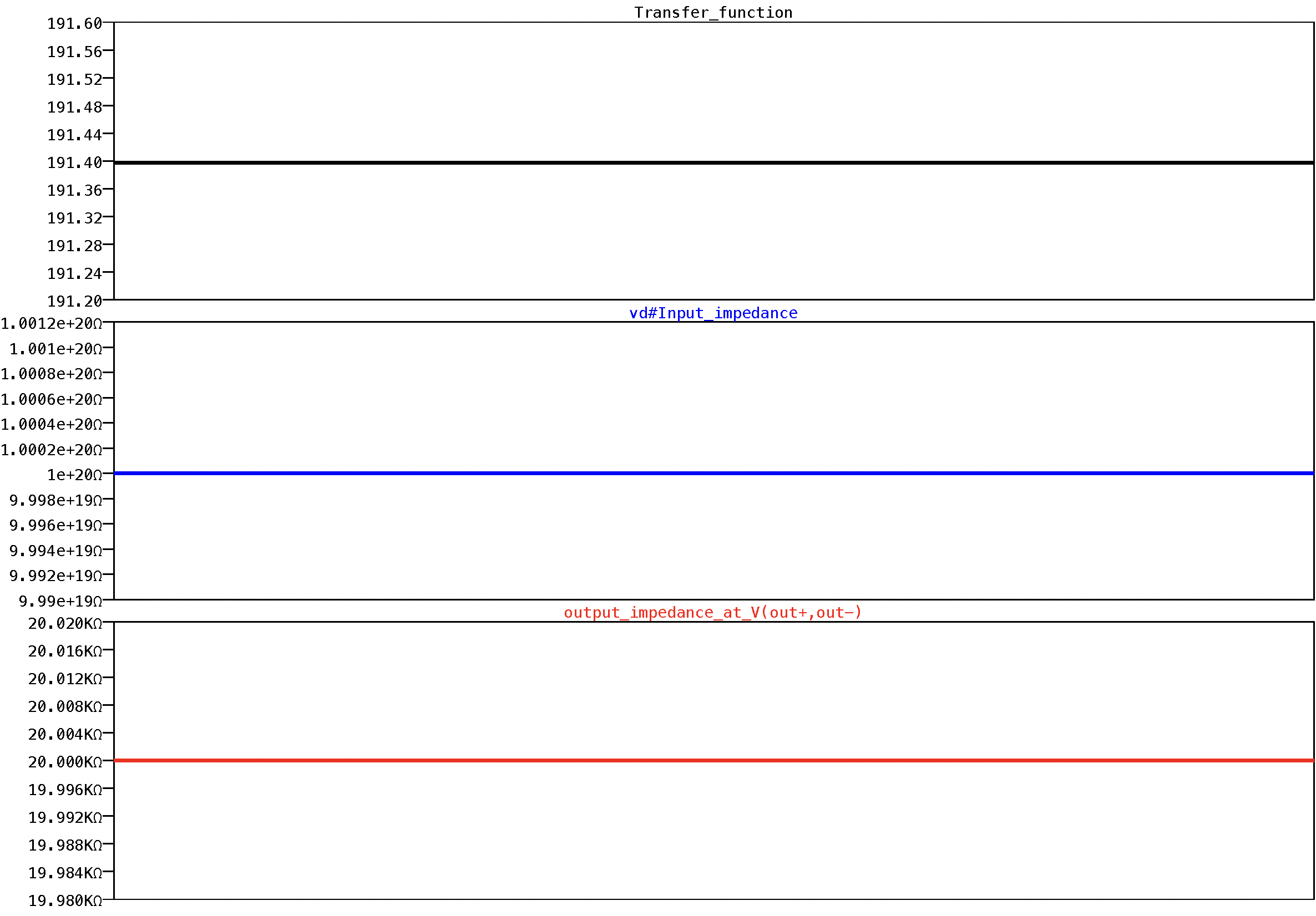
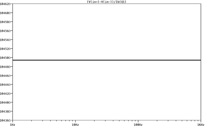
As is evident from the above data, the input-output voltage gain is 191.40 V/V, input resistance is 1020 Ω and output resistance is 20 kΩ. Unfortunately, with this multiple source arrangement, the resistance seen by the input source Vd is just the resistance seen looking into the open circuit port of the VCVS. Hence, the reason for the very large value of 1020 Ω. We therefore require another means of obtaining the small-signal resistance seen looking into this differential amplifier. If we consider applying a 1 V AC signal across Rd, then this signal will also appear across the input terminals of the differential pair. By calculating the current that flows into the terminals of the differential pair, the input resistance can be found by equating the ratio of the input voltage to the input current. Redefining the Spice directive to an .AC command, such as the following:
|
.AC LIN 1 1Hz 1000Hz |
results in an input resistance of about 10.45-k Ω, as seen from the plot below:
One could have found a similar result by altering the DC voltage of the Vd source from 0 V to, say 1 mV and use a .OP Spice directive command and get a similar result. However, this result would not be considered a small-signal result, as it involves a nonlinear DC calculation. Nonetheless, the .OP analysis provides a listing of each transistor small-signal model. These are listed below:
|
Semiconductor Device Operating Points:
--- Bipolar Transistors --- Name: q2 q1 Model: npn_transistor npn_transistor Ib: 4.95e-06 4.95e-06 Ic: 4.95e-04 4.95e-04 Vbe: 6.28e-01 6.28e-01 Vbc: -1.00e+01 -1.00e+01 Vce: 1.07e+01 1.07e+01 BetaDC: 1.00e+02 1.00e+02 Gm: 1.91e-02 1.91e-02 Rpi: 5.22e+03 5.22e+03 Rx: 0.00e+00 0.00e+00 Ro: 0.00e+00 0.00e+00
|
Using the expressions given in Table 6.1, we can expect that this amplifier will have a differential gain of 191.0 V/V and an input differential resistance of 10.44 kΩ, values that are very close to those computed directly by LTSpice.
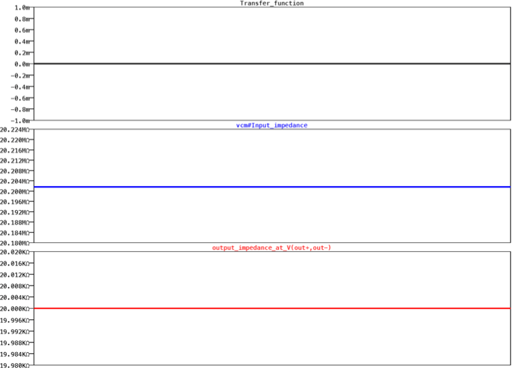
To further analyze the differential amplifier shown in Fig. 6.7, let us compute the common-mode voltage gain and common-mode input resistance using Spice. One proceeds in exactly the same way that the differential-mode analysis was performed above using the .TF command, except that we change the source reference from Vd to Vcm as shown below:
.TF V(OUT+,OUT-) Vcm
The results of this analysis are plotted below:
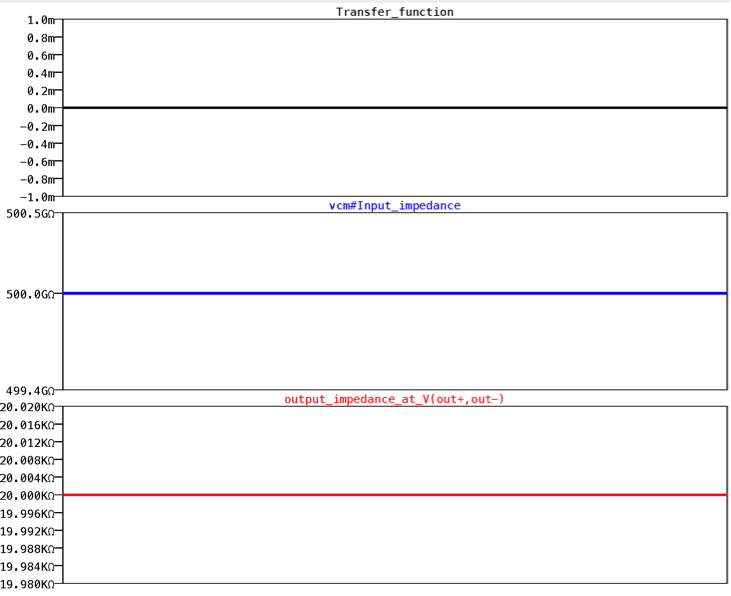
Here we see that the common-mode voltage gain of this amplifier is exactly zero, which agrees with what one would expect given that the resistance in the two collectors are equal. Note that the input resistance is 500-GΩ rather than the theoretically expected value of infinity; a numerical artifact of LTSpice. We also note that the output resistance computed during this analysis is identical to that found during the previous analysis for differential-mode behavior.
|
|
|
(a) |
|
|
|
(b)
|
|
Fig.6.9: (a) Including a 200 kΩ current source resistance in the differential amplifier of Fig. 6.7. (b) The schematic captured by LTSpice with multiple Spice directives. |
In the above analysis, we assumed that the differential pair was biased by an infinite-output-resistance current source I. In practise, an infinite-output-resistance current source cannot be achieved. It is therefore imperative to repeat the above analysis including this current-source resistance, such as that shown in Fig. 6.9, and thus verify whether the expressions seen listed in Table 6.1 remain accurate. After all, in the development of most of these formulae, the current-source resistance was assumed infinite. Here we shall assume a current-source resistance of 200 kΩ.
We begin by modifying the circuit schematic of the differential amplifier circuit of Fig. 6.8 by including the 200 kΩ current-source resistance as shown in Fig. 6.9(b) and re-running the .TF command, resulting in the following:
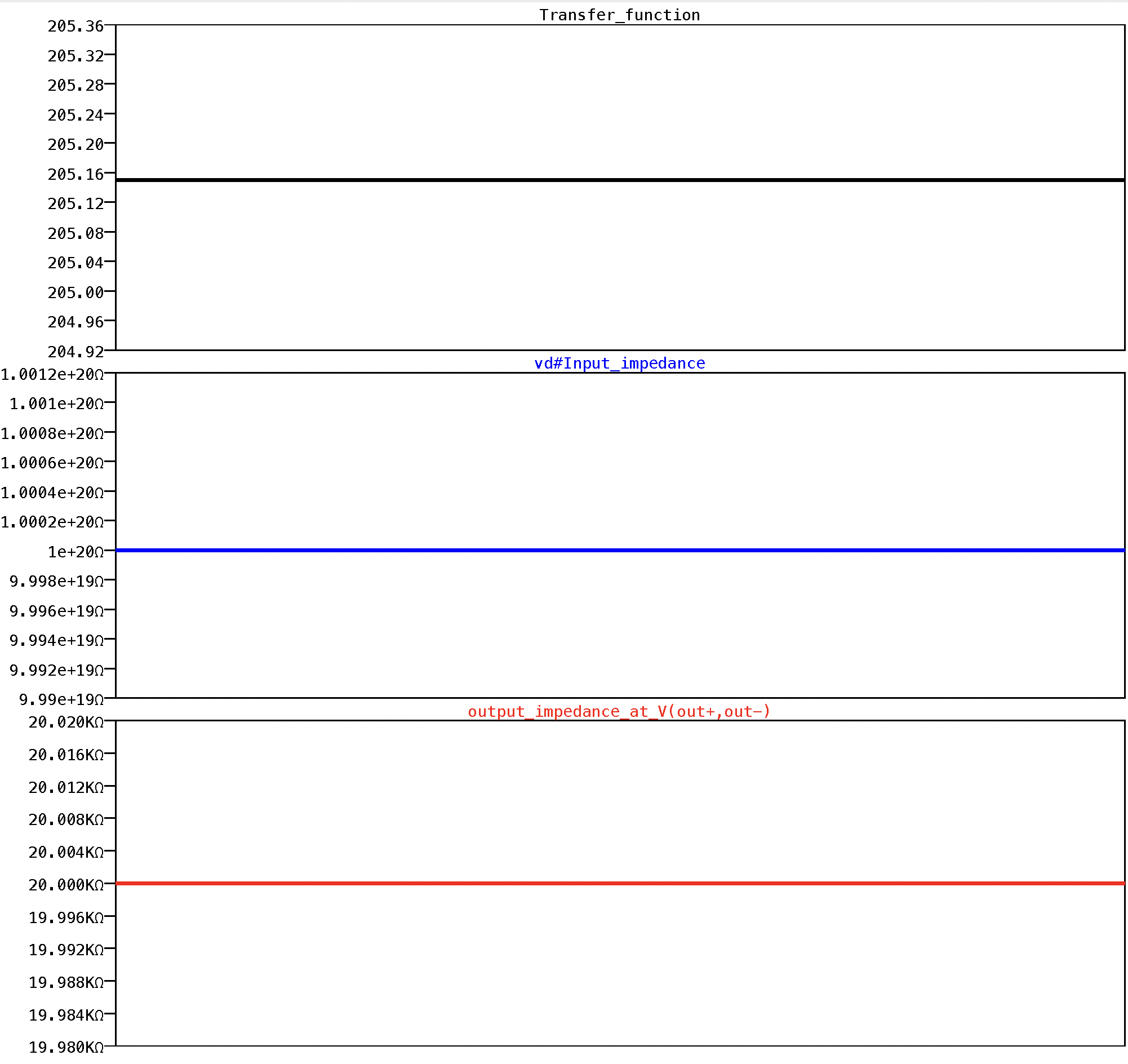
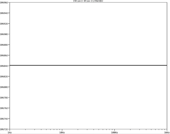
As is evident from the above data, the input-output voltage gain is 205.16 V/V, input resistance is 1020 Ω and output resistance is 20 kΩ. These results are very close to the previous case when the resistance of the current source was assumed infinite. The small differences in these small-signal results are due not directly to the presence of the source resistance R, but rather, because the addition of the source resistance alters the DC bias conditions of the two transistors. Once again, the input resistance value displayed here is not valid. To acquire a value for the input resistance, the previous .AC analysis command is run, leading to the following AC frequency plot:
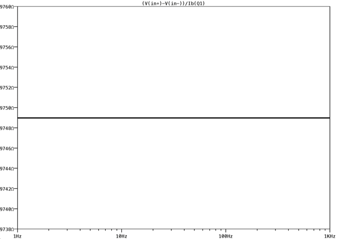
As is evident, the input differential resistance was found to be around 9750 Ω.
We can proceed and modify the Spice directive to compute the common-mode input equivalent circuit, as was done before, and arrive at the following plot:
Using the formulas given in Table 6.1, together with the small-signal model parameters for Q1 and Q2, we would obtain exactly the same results as those computed by Spice.
In each of the analyses performed above in this section, the Early effect was neglected. Let us now consider the situation where the Early voltage of each transistor of the differential pair is 100 V. We shall maintain the current-source resistance at 200 kΩ. The transistor model for this situation is very similar to that shown in Fig. 6.8 and 6.9, with the model statement for each transistor modified according to:
.model npn_transistor npn ( Is=14fA Bf=100 VAf=100V ).
The results of both the differential-mode and common-mode analysis computed by LTSpice are:
|
Differential-Mode Analysis: |
Common-Mode Analysis:
|
|
|
|
|
|
|
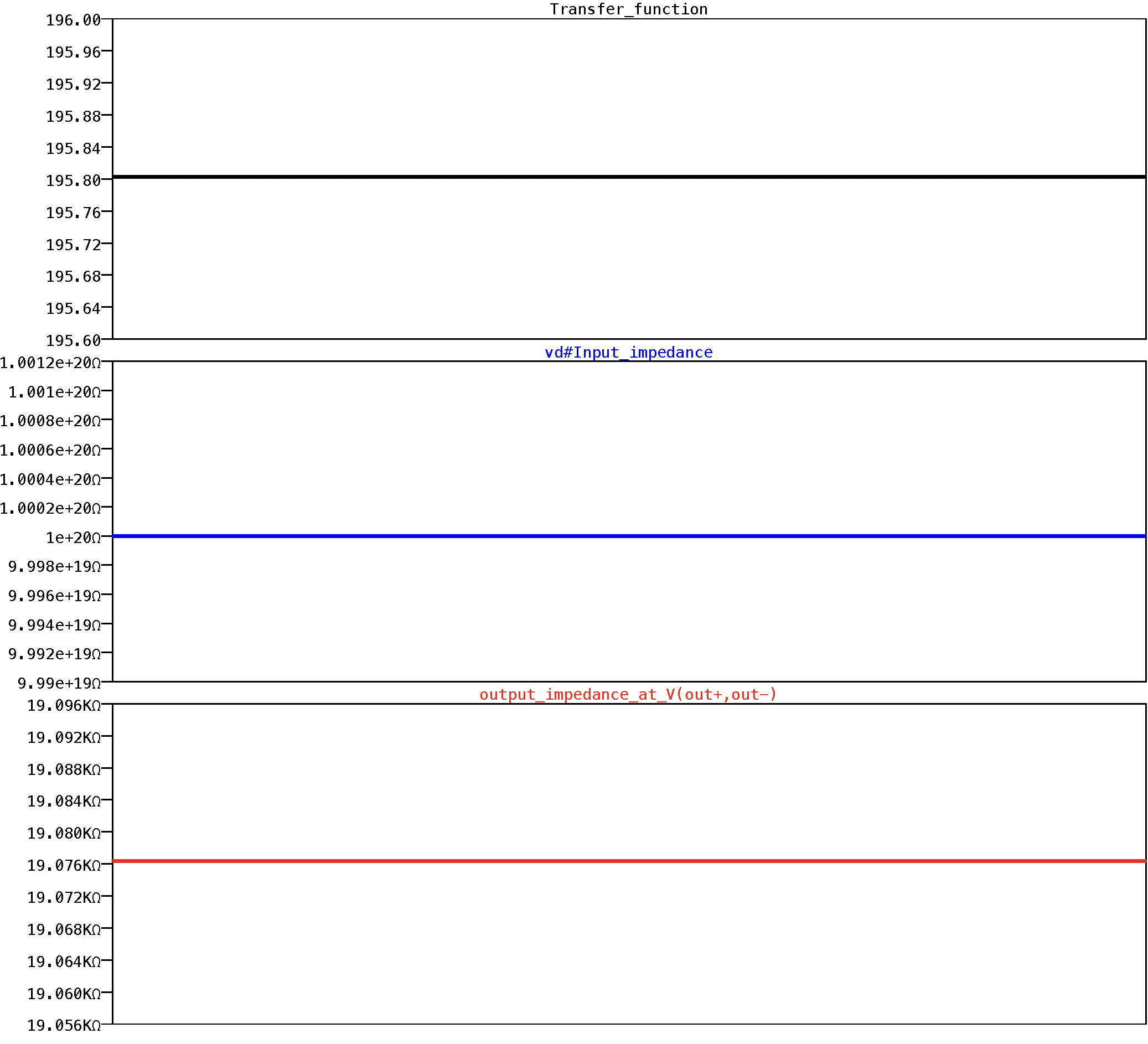
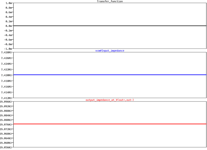
As is evident from these results, the differential-mode voltage gain is 182.7 V/V. The input differential resistance is calculated from the input current to be 10.684 kΩ. The common-mode voltage gain is, for all practical purposes, zero and the input common-mode resistance is 7.42 MΩ.
As a means of verifying the formulae given in Table 6.1 under the conditions of finite Early voltage, we also list the parameters of small-signal model computed by LTSpice below:
|
Semiconductor Device Operating Points:
--- Bipolar Transistors --- Name: q2 q1 Model: npn_transistor npn_transistor Ib: 4.84e-06 4.84e-06 Ic: 5.31e-04 5.31e-04 Vbe: 6.28e-01 6.28e-01 Vbc: -9.69e+00 -9.69e+00 Vce: 1.03e+01 1.03e+01 BetaDC: 1.10e+02 1.10e+02 Gm: 2.05e-02 2.05e-02 Rpi: 5.34e+03 5.34e+03 Rx: 0.00e+00 0.00e+00 Ro: 2.07e+05 2.07e+05 |
Substituting the above parameter values into the expressions for Ad, Rid, ACM and RiCM seen listed in Table 6.1, and approximating ru by 10 roβ, we obtain the following estimates of the amplifiers small-signal behavior: Ad=182.8 V/V, Rid=11.52 kΩ, ACM=0 and RiCM=6.75 MΩ. Comparing these with those computed directly by LTSpice we see that we are in good agreement with all of them except RiCM. The formula for RiCM seen listed in Table 6.1 seems to underestimate the actual input common-mode resistance by about 14%. One possible source of error may be due to our approximation of ru by 10 roβ.
|
Table 6.2: Comparing the small-signal parameters of the differential amplifier shown in Figs. 6.7 and 6.9 as calculated by hand analysis and those computed by Spice.
|
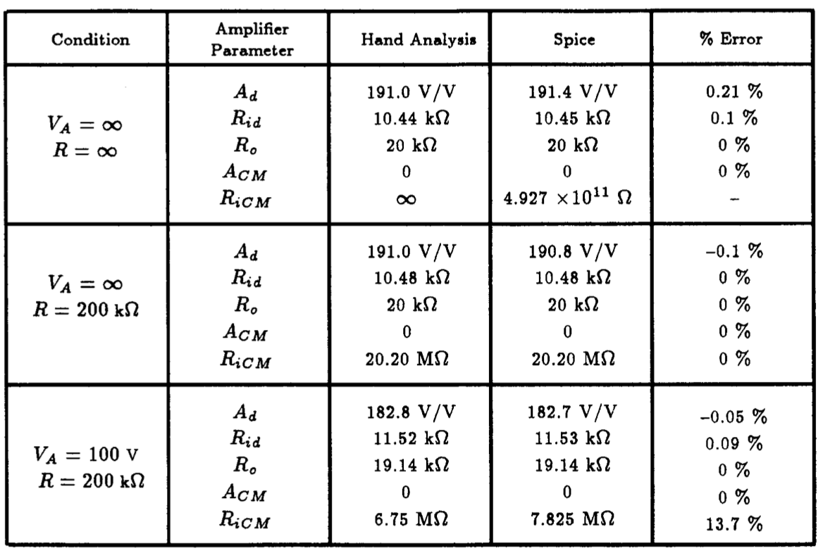
To summarize the results of this section we have compiled a list in Table 6.2 that compares the results computed directly by LTSpice to those computed using the formulae presented in Table 6.1. Furthermore, the rightmost column of this table lists the relative error in percent. As is evident, the results predicted by the formulae of Table 6.1 agree quite well with the results computed by LTSpice. We can therefore conclude that when given good estimates of the small-signal model parameters, the formulae of Table 6.1 will predict quite accurately the small-signal differential and common-mode voltage gain of a differential amplifier and its corresponding input resistances.
6.3 Small-Signal Analysis of the Differential Amplifier: Asymmetric Conditions
The previous section assumed that many of the components in the differential amplifier of Figs. 6.7 or 6.9 were matched. In practise this is rarely the case. In this section we shall investigate the effect of asymmetric circuit conditions on amplifier behavior. Specifically, we are interested in observing the effect of variations, or mismatches, in collector resistances, transistor saturation (scale) currents, and transistor beta's on circuit behavior.
|
Fig.6.10: Differential amplifier with current source output resistance subject to ±5% uniform random variations in the collector resistors.
(a)
(b)
Fig. 6.11: Highlighting the several parameters of the differential amplifier shown in Fig. 6.9 subject to collector resistance random mismatches having a ±5% uniform distribution: (a) the input-referred offset voltage, and (b) common-mode gain – derivative of the common-mode transfer characteristics.
|
Input Offset Voltage
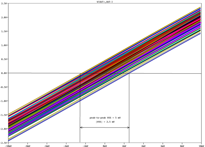
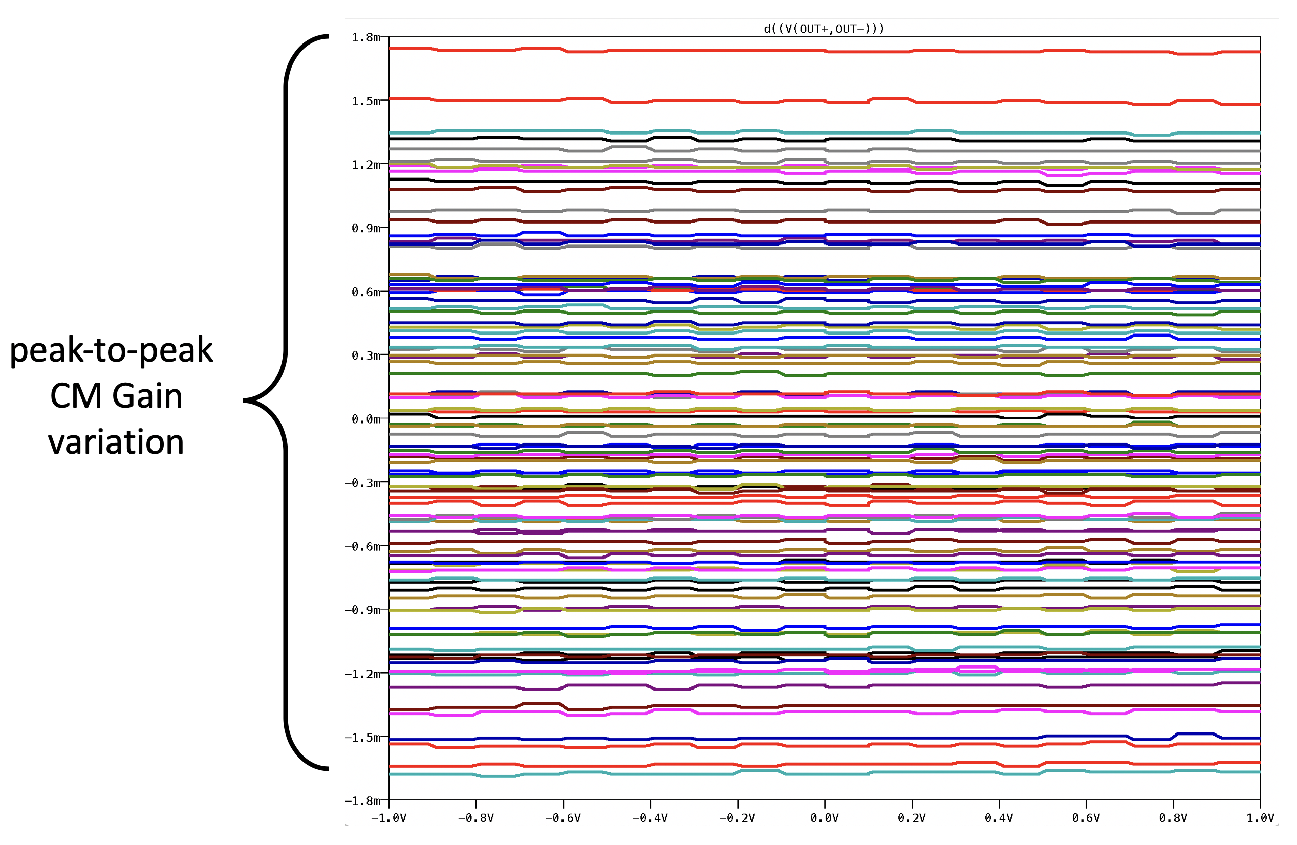
To begin with, let us consider using LTSpice to determine the input offset voltage VOS for the differential amplifier shown in Fig. 6.9 assuming that each collector resistor experiences a random change of ±5% drawn from a uniform distribution centered around the nominal resistance of 10 kΩ. The reader will recall in Chapter 4 and 5, a Monte Carlo analysis was performed to collect statistical data on the effect of these random variations. The same will be performed here. The analysis that we are requesting here is a DC sweep of the input differential voltage Vd. The range of our sweep is limited to be between -10 mV and +10 mV. The range of this sweep was determined by considering the formula for input offset voltage VOS in Table 6.1. Given that DRC/RC = ±5% = 10%, we can expect an input offset voltage having a peak-magnitude of 2.6 mV. Thus, we decided that our sweep should not exceed this by very much so that the zero crossings can be easily seen. The LTSpice captured circuit schematic for this particular example is shown listed in Fig. 6.10. Also included in the LTSpice circuit schematic is another DC sweep command use to compute the common-mode voltage transfer characteristics. At this time, it is deactivated. We’ll return to this in a moment.
The results of the DC sweep of the input differential voltage are shown in Fig. 6.11(a) for a ±5% variation in the collector resistance. Here we see that the transfer function curve vo vs. Vd for this particular case (as there are other cases also shown in this figure), no longer passes through the origin. Instead, careful probing using the waveform viewer facility of LTSpice indicates that the input-referred offset voltage varies with a peak-to-peak variation of about 5 mV. Interestingly enough, this corresponds exactly with the magnitude of the value predicted by the formula given in Table 6.1. The DC sweep of the common-mode voltage Vcm is activated and executed. Rather than plot the transfer characteristic vo vs vcm for different collector resistances, the derivative dvo/dvcm is plotted instead in Fig. 6.11(b). The derivate operation is a built-in function of the LTSpice waveform viewer. The results of Fig. 6.11(b) show that the common-mode gain varies from -1.8mV/V to +1.8 mV/V. According to the common-mode gain formula provided in Table 6.1, a peak-magnitude gain of 2.5 mV/V is predicted. This result is reasonably close to that found from the Monte Carlo simulation using ±5% collector resistors.
|
|
|
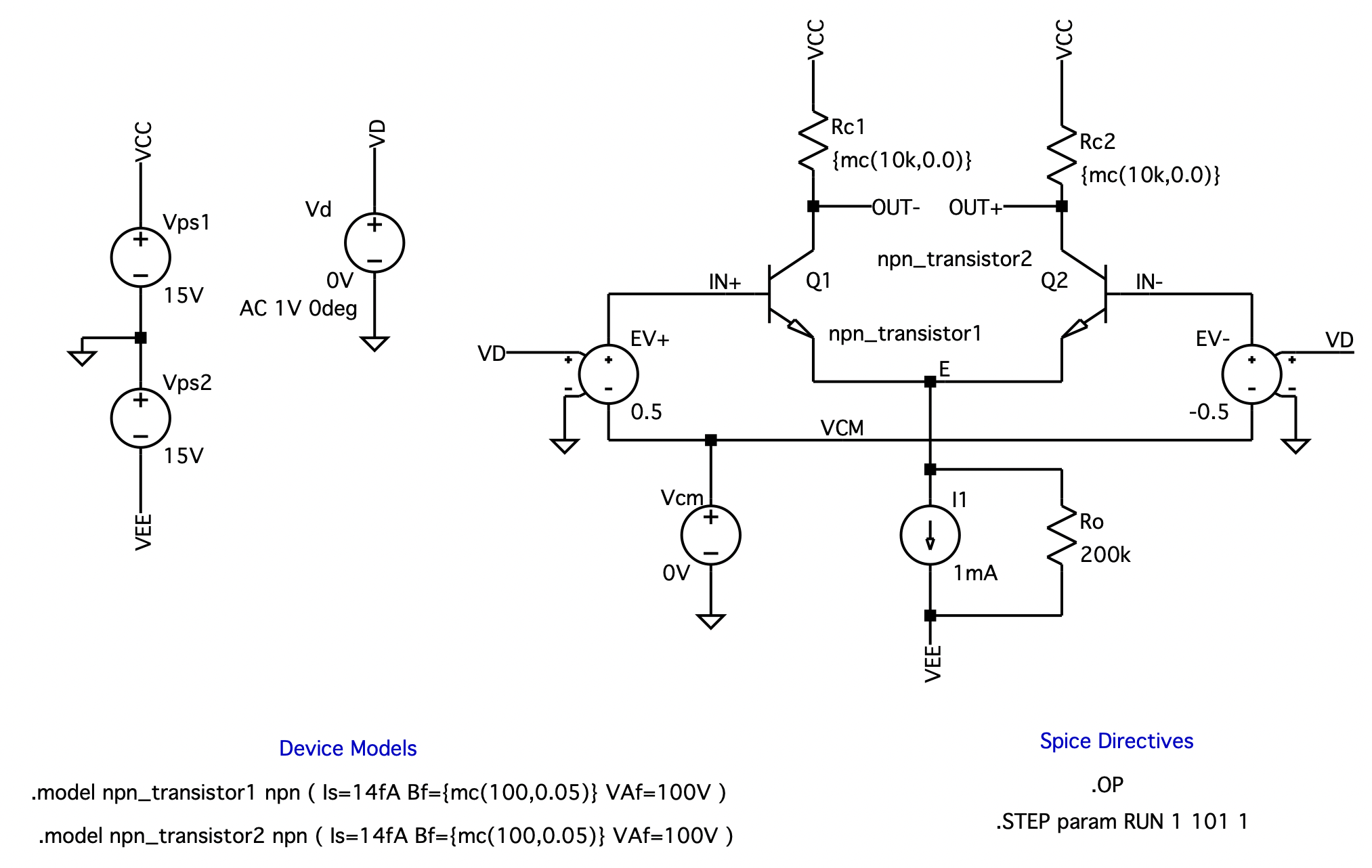
Fig.6.12: Differential amplifier with current source output resistance subject to a ±5% mismatch in the saturation current of transistor Q1 and Q2. Note that each transistor is assigned a specific device model.
|
|
Fig.6.13: Input-referred offset voltage of the differential amplifier subject to ±5% mismatch in the saturation current of Q1 and Q2.
|
We can repeat the above analysis and determine the effect that a ±5% difference between the saturation currents IS of the two transistors on the amplifiers input offset voltage. To do so, each transistor must be assigned a separate model, with the saturation current assigned a random variable as follows:
.model npn_transistor1 npn ( Is={mc(14f,0.05)} Bf=100 VAf=100V )
.model npn_transistor2 npn ( Is={mc(14f,0.05)} Bf=100 VAf=100V )
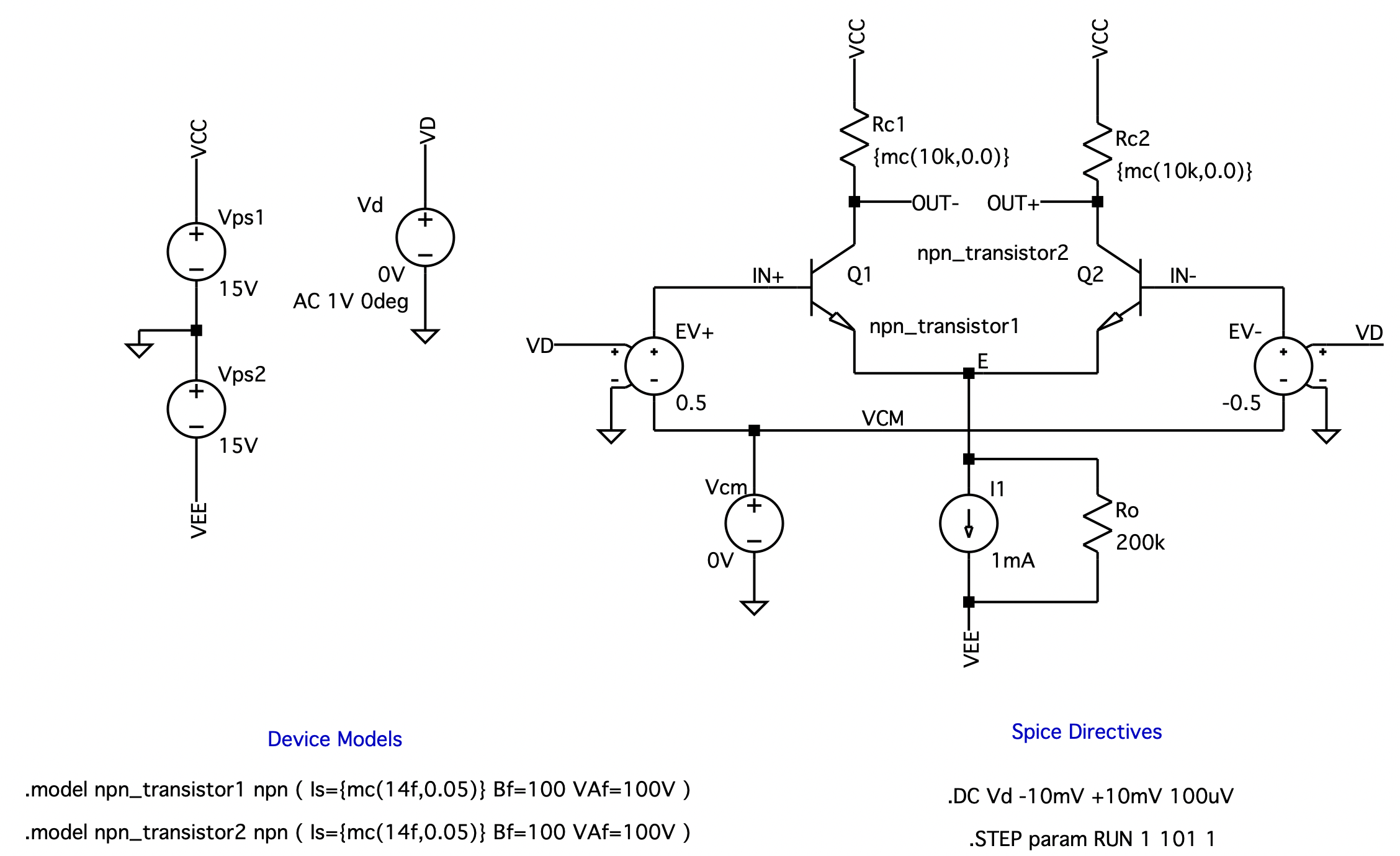
The LTSpice circuit capture with Monte Carlo Spice directive for this particular case is provided in Fig. 6.12. Here a dc sweep of the differential-input transfer characteristic is generated over 100 separate random runs. The results of this analysis are shown in Fig. 6.13 of the output voltage versus input differential voltage. Using the waveform viewer, we can determine that the peak-to-peak input-referred offset voltage is 4.76 mV. According to the formula given in Table 6.1, we can expect an input offset voltage having a magnitude of 2.6 mV, or equivalently, a 5.2 V peak-to-peak value. Clearly our estimate of the input offset voltage prediction agrees with that obtained with LTSpice.
|
|
|
Fig.6.14: Differential amplifier with current source output resistance subject to a ±5% mismatch in transistor beta’s. Note that each transistor is assigned a specific device model.
|
|
|
Input Bias and Offset Currents
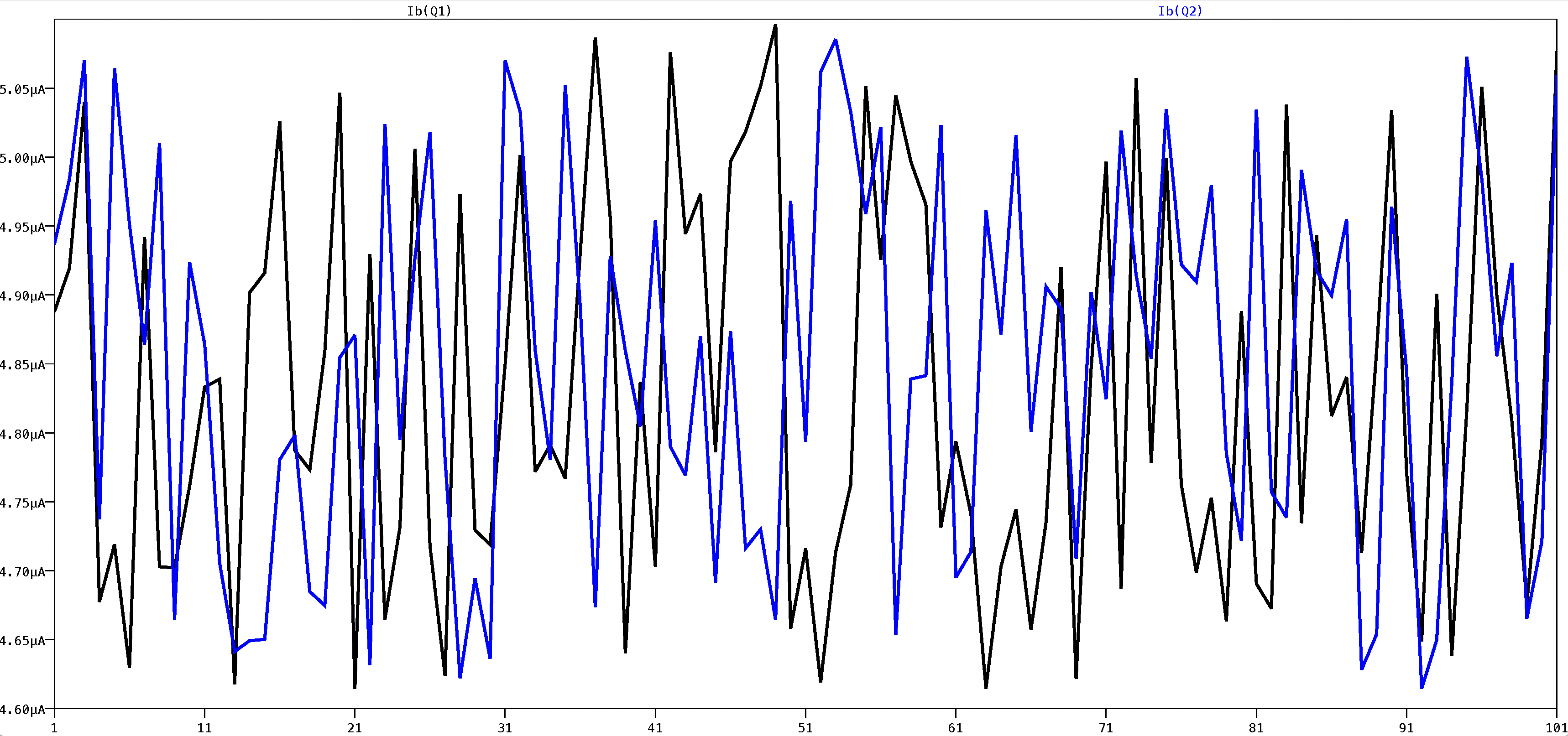
Mismatches in transistor beta's result in different base currents, which, in turn, give rise to differences in the input bias currents to the amplifier. To demonstrate this, consider modeling the beta of Q1 and Q2 in the differential amplifier with a uniform distribution centered around 100 but bounded by ±5% of this value. Each transistor would require its own model statement, such as
.model npn_transistor1 npn ( Is=14fA Bf={mc(100,0.05)} VAf=100V )
.model npn_transistor2 npn ( Is=14fA Bf={mc(100,0.05)} VAf=100V )
As the input bias currents are of interest, an .OP command would be sufficient to capture this information. The LTSpice captured circuit is shown in Fig. 6.14 and the variation in the bias currents are displayed in Fig. 6.15. As one can see, the behavior of the base currents of Q1 and Q2 vary in much the same way., both experiencing a peak-to-peak variation of 472 nA. It is interesting to note that the formula provided in Table 6.1 generates a value very close to that found by LTSpice.
|
|
|
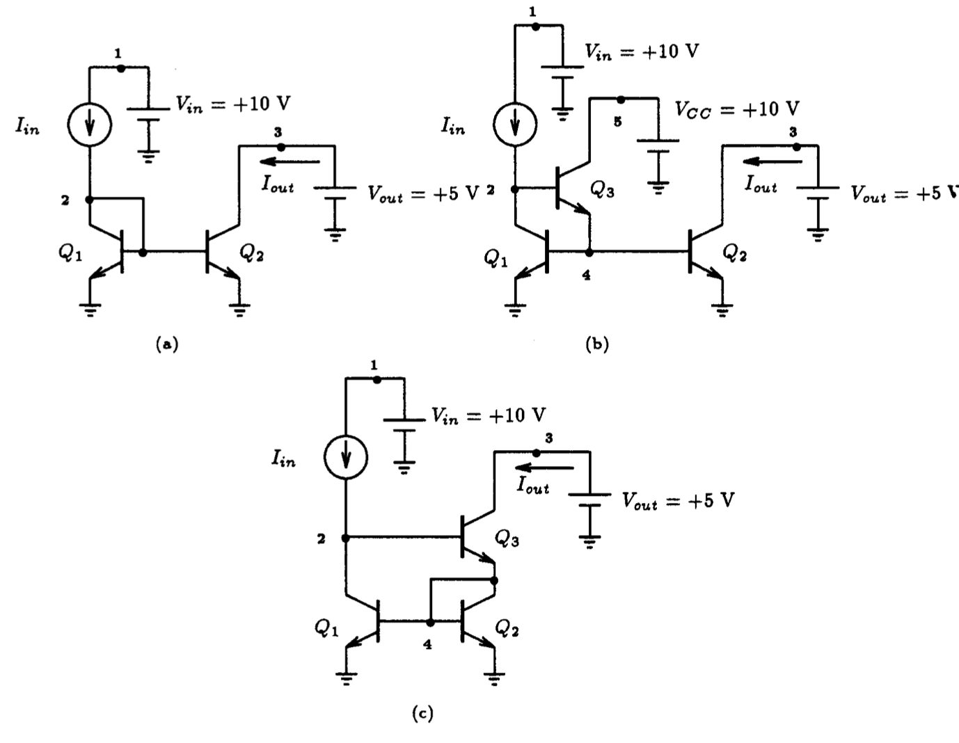
Fig. 6.16: Various current mirror circuits: (a) A simple two-transistor current-mirror circuit. (b) A current mirror with base-current compensation. (c) The Wilson current mirror circuit. Various voltage sources are used to monitor different branch currents.
|
6.4 Current-Mirror Circuits
Current mirror circuits play a very important role in the design of IC current sources and current-steering circuits. A current mirror circuit consists of two or more transistors arranged in such a way that at least two transistors in the circuit have their bases and emitters connected together causing them to have equal vBE's. There are many different current mirror circuits, each suitable for a different application. In the following we shall investigate several widely used current mirror circuits: A two-transistor current mirror, herein referred to as the simple current mirror, the simple current mirror with base-current compensation, and the Wilson current mirror. Each of these is depicted in Fig. 6.16. In our investigation, we shall judge the behavior of these current mirrors based on their: (a) current gain accuracy, (b) output resistance, (c) minimum output voltage, and (d) input current range. Another important aspect of a current mirror circuit is their frequency response behavior. However, we defer discussion of this topic until the next chapter.
|
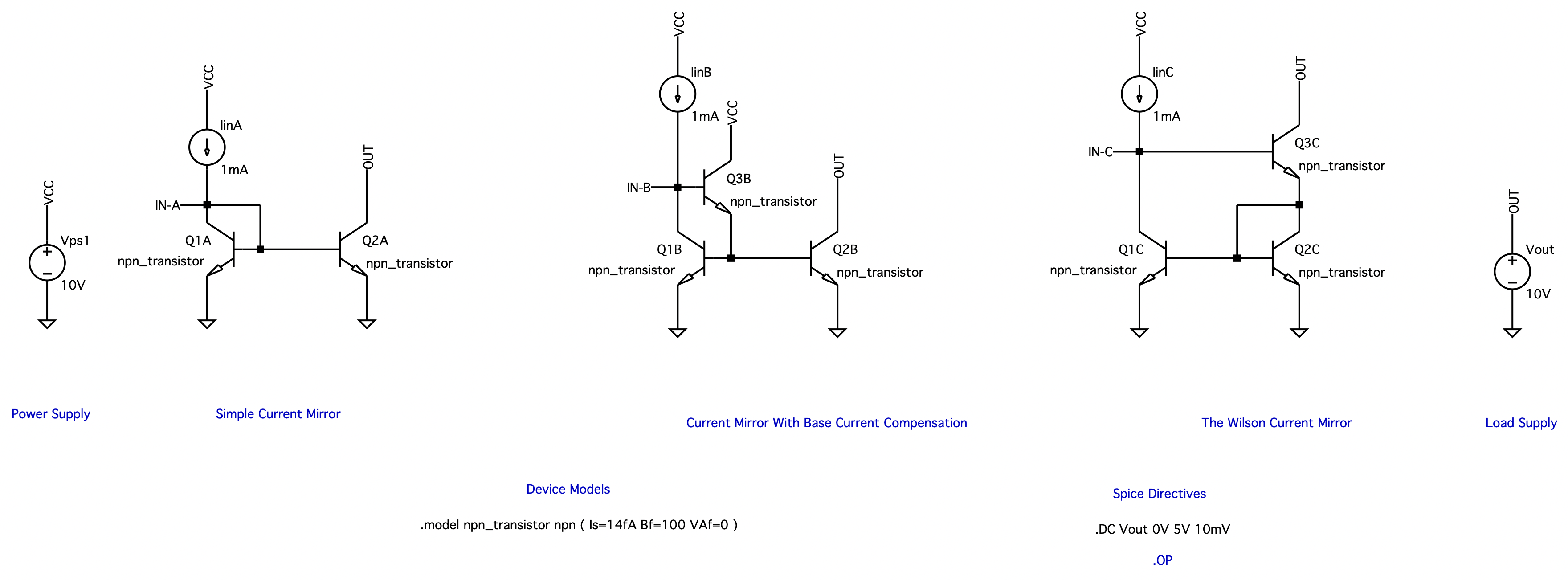
Fig. 6.17: The circuit schematic for the three current mirror circuits of Fig. 16.6 captured in LTSpice for calculating the current transfer ratio Iout / Iin. The npn transistor Early Voltage will be assume infinite for the first test.
|
|
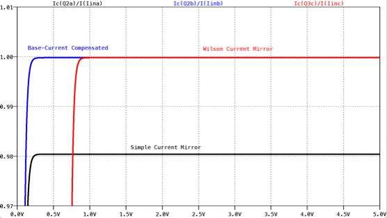
Fig. 6.18: Comparing the current transfer characteristics of the various current mirror circuits shown in Fig. 6.17 as a function of the output voltage. Only the effects of transistor base currents are considered in this analysis (i.e., VA=¥).
|
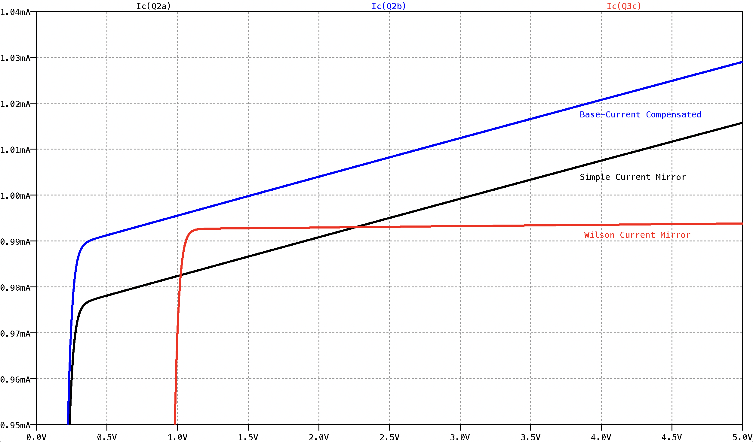
Fig. 6.19: The Iout versus Vout characteristics of the various current mirror circuits shown in Fig. 6.17. The effect of transistor Early voltage has been included in this analysis.
|
|
|
|
Fig. 6.20: Demonstrating the variations in the current transfer ratio of the Wilson current mirror over an input current range of 1 µA to 1 mA.
|
Current-Gain Accuracy:
The current-gain accuracy is an indication of how significantly the transistor base currents affect the operation of the current mirror circuit. The current gain is the ratio of the output current to the input current (Iout/Iin). In hand analysis, the current gain is usually evaluated with the Early effect neglected. Obviously, the more ideal a current mirror is, the closer this ratio is to unity. For the simple current mirror, it has been shown by hand analysis that the current transfer ratio is 1 / (1 + 2/β). Conversely, the current transfer ratio for the remaining two current-mirror circuits shown in Fig. 6.16 can be approximated by 1 / (1 + 2/β2). For β=100, the simple current mirror has a current transfer ratio of 0.9803 A/A, whereas the other two mirror circuits have a ratio much closer to unity, of value 0.9998 A/A. Clearly, the simple current mirror is not very accurate.
With the aid of LTSpice, let us observe the current transfer ratio of the current-mirror circuits shown in Fig. 6.16 for various output voltage levels. We shall consider that the transistor is ideal except that it has a finite beta equal to 100. The Early Voltage for the npn transistor will be initially set to infinity (i.e., VAf=0). Modeling the transistor in this way will enable us to compare the result generated by LTSpice with that calculated by hand. Furthermore, we shall assume that each transistor of the mirror circuit is integrated on a common p-type substrate. As such, the common substrate connection must be defined. This is usually necessary in order to obtain matched devices without trimming. To ensure proper isolation, the pn junction formed by the substrate is reverse biased by connecting the substrate to the lowest potential in the circuit. In this particular case it would be the ground node (node 0).
Let us consider capturing the three circuits of Fig. 6.16 in LTSpice. These are shown in Fig. 6.17 as a single schematic entry. This will allow for comparisons between the three current mirrors. Each current mirror is supplied with a 1 mA input current source with one side connected to a 10 V DC voltage source (node labeled as VCC). The output terminal of each current mirror is connected to a separate 5 V DC voltage source. This voltage source acts to simulate various load conditions. A DC sweep of the output voltage source is to be performed over a voltage range varying between 0 and 5 V in increments of 10 mV using the following .DC sweep directive:
.DC Vout 0V 5V 10mV
A DC operating point analysis is also included in this LTSpice command window but is presently inactive (blue text). The results of this LTSpice analysis are shown in Fig. 6.18. Here we have plotted the output current normalized to the input current level of 1 mA. This operation was performed directly with the Waveform Viewer facility of LTSpice. Furthermore, with the cursor feature of the Waveform Viewer, the base-current compensated mirror circuit and the Wilson current mirror circuit have nearly ideal current gain at 0.9998 A/A, whereas, the current transfer ratio for the simple current mirror was found to be 0.9804 A/A. All three sets of results agree with those found with the above hand calculations. We also notice from the current transfer characteristics shown in Fig. 6.18 that when the output voltage goes too low, the current transfer ratio drops significantly towards zero. This suggests that the current mirror has a limited range of operation. We shall have more to say about this in a moment when we consider a more sophisticated model for the transistor.
Output Resistance:
Based on the above analysis, one might be tempted to conclude that both the base-current compensated current mirror and the Wilson current mirror could be used interchangeably, given that their current gain accuracies are identical. Unfortunately, this is not the complete picture because the analysis above ignored the Early effect. As we shall see, the current gain ratio of a current mirror can be adversely affected by the Early voltage of a transistor, thus altering our conclusion about which circuit is the better current mirror.
To see this, let us modify the model statement for the npn transistor used in the LTSpice schematic for each of the current mirror circuits by the following transistor model statement:
|
.MODEL npn_transistor NPN (IS=5E-17 BF=147 VAF=80 IKF=4.3E-3 ISE=8E-18 NE=1.233 + BR=1.9 VAR=11 IKR=6E-4 ISC=5E-16 NC=1.08 RE=12 RB=1200 RBM=200 RC=25 + CJE=58E-15 VJE=0.83 MJE=0.35 CJC=133E-15 VJC=0.6 MJC=0.44 XCJC=1 + CJS=830E-15 VJS=0.6 MJS=0.4 ISS=1E-16 FC=0.85 TF=60P XTF=48 ITF=3E-2 + TR=10N EG=1.16 XTI=3 XTB=1.6)
|
This Spice model was chosen here because it is representative of a typical small-sized integrated npn transistor found on a bipolar semi-custom analog transistor array manufactured by the Gennum Corporation [Gennum Data Book, 1991]. We shall maintain the input current to each mirror at 1 mA. Typically, these transistors have a forward Bac of approximately 90 at a bias current of 1 mA and an Early voltage in the neighborhood of 80 V. One should bear in mind that current mirror circuits are generally called on to mirror a wide range of currents and not just a single current level. We shall address this issue below in the subsection entitled: Input Current Range.
Submitting the revised schematic for the three current mirrors for analysis, a plot of the output current as a function of the output voltage is shown in Fig. 6.19. As is evident, the behavior of the base-current compensated mirror circuit and the Wilson current mirror circuit now differ significantly. The Wilson current mirror has an i - v behavior that is very much independent of the output voltage, i.e., near zero slope. On the other hand, both the base-current compensated mirror and the simple current mirror circuit have behavior that depends strongly on the output voltage. To quantify the output resistance of each of these current mirrors, we can simply estimate this from the reciprocal of the slopes of the i - v characteristics of each mirror in their linear regions. The cursor facility of the waveform viewer will be used to obtain these slopes directly from the graph shown in Fig. 6.19. In the case of the simple current mirror and the base-current compensated mirror circuit, the output resistance is approximately 120 kΩ. The Wilson current mirror has a much higher output resistance of about 3.48 MΩ.
According to small-signal analysis, the output resistance of the simple current mirror, and the base-compensated current mirror, is simply the incremental resistance ro of the output transistor (i.e., Q2 in the circuits of Fig. 6.16(a) and (b)). However, according to the Early voltage and the transistor bias level, we estimate the incremental output resistance of this transistor to be VA / I = 80 V / 1 mA = 80 kΩ. (The results of a .OP command also confirm something very close to this value). However, the LTSpice result indicate mirror output resistance of 120 kΩ. Thus, some other effect must be playing a major role in increasing the output resistance of these current mirrors. A detailed investigation reveals that the integrated npn transistor used in our simulations has a 12-Ω resistor in series with the emitter (See the model statement for this transistor, given above). Although, the value of this resistor seems small, its effect on the output resistance of the current mirror is significant.
According to small-signal analysis, the resistance seen looking into the collector terminal of a transistor, denoted as ro, with emitter resistance RE is given by
(6.1)
![]()
In the situation described above for the two simple current mirror circuits, RE of 12 Ω dominates the parallel combination of RE||rp because rp is in the kΩ range (i.e., rp = B/gm where gm=IC/VT =1 mA /25 mV = 40 mA/V). Thus, according to Eqn. (6.1), the output resistance of this mirror is calculated as follows:
![]()
Clearly, our estimate of the output resistance is now in-line with that observed through computer simulation of 120 kΩ.
For the case of the Wilson current mirror, its output resistance is given by
(6.2)
![]()
Attaching a numerical value of 90 to beta and 80 kΩ to ro, suggests that the output resistance is approximately 3.6 MΩ. This, then, agrees quite closely with the value of the output resistance obtain through LTSpice of 3.48 MΩ. The effect of the emitter resistance of each transistor is much greatly reduced due to the feedback action of the three-transistor loop which forms the Wilson current mirror circuit.
Based on the above observations of current mirror accuracy and output resistance, one would probably prefer the Wilson current mirror over the other two current mirror circuits shown in Fig. 6.16.
Minimum Output Voltage:
A drawback to the Wilson current mirror is that it requires a relatively high output voltage to operate in the linear region (1.12 V as opposed to 0.36 V for the other two circuits; see Fig. 6.19). When used as an active load in an amplifier configuration, the required voltage reduces the range of the output voltage swing and is therefore not desirable.
Input Current Range:
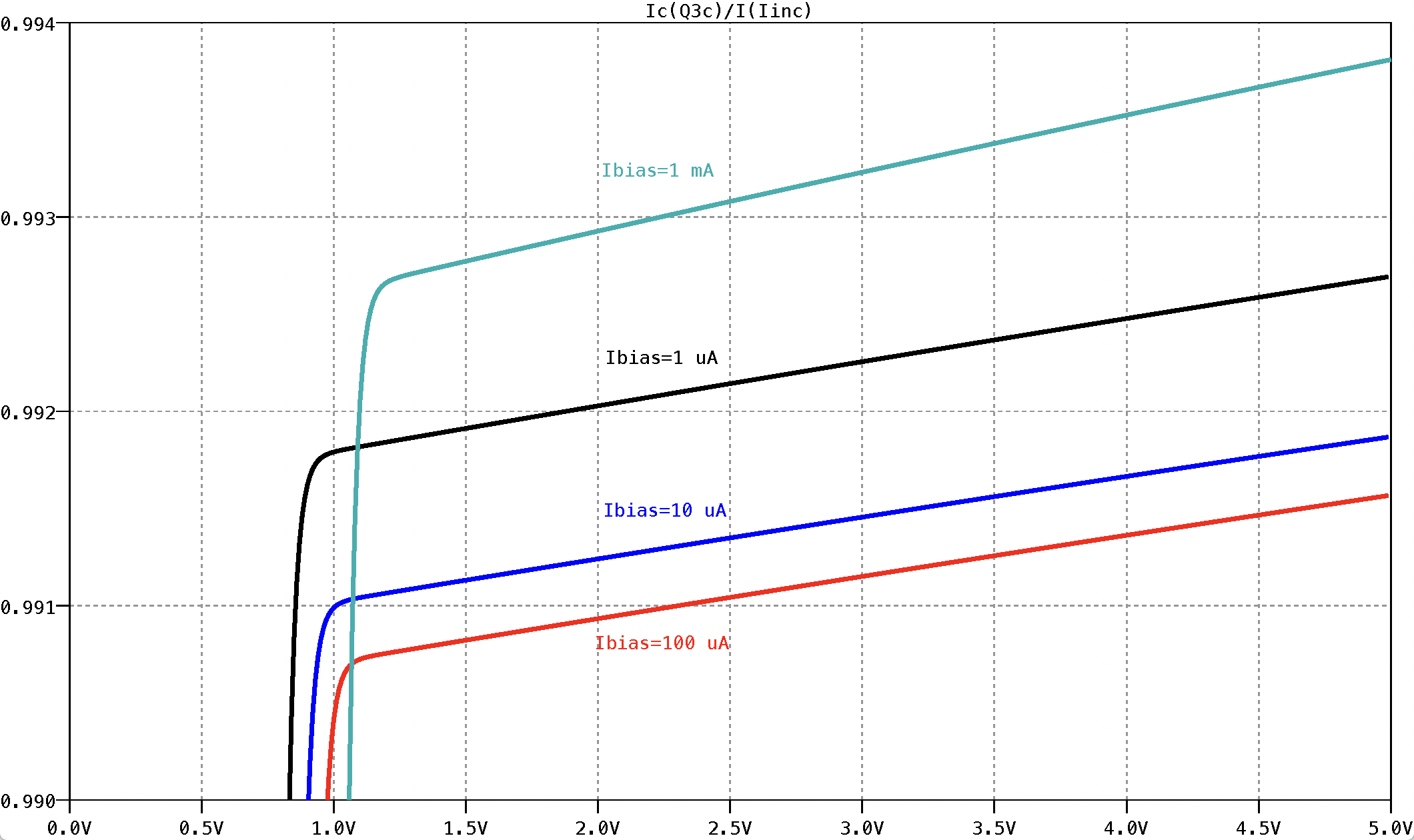
Current mirrors are expected to operate over a wide range of input current levels. In the above analysis, the various attributes of the different current mirror circuits were all evaluated at a single input current level of 1 mA. We shall now explore the performance of the Wilson mirror at various input current levels using the Gennum IC model described above. Specifically, we shall evaluate its i - v characteristic at input current levels of 1 𝜇A, 10 𝜇A, 100 𝜇A and 1 mA using the following .STEP directive:
.STEP param Ibias LIST 1u 10u 100u 1000u
The results of this analyses are shown plotted in Fig. 6.20. Rather than plot the wide range of output currents on a single graph, where much detail would be lost with the scale used there, we instead plot the ratio of the output current to the input current, Iout / Iin, as a function of the output voltage. In this way, the same scale can be used for all input current levels and comparisons can easily be made. The output resistance and the minimum output voltage can be derived from the data contained in this graph.
Over an input current range of 1 𝜇A to 1 mA, the minimum output voltage can be seen to vary between 0.82 V and 1.04 V. In addition, over this same current range, we see that the slopes of Iout/Iin versus Vout curves are quite similar ranging between 210 to 292 𝜇A/A per volt. Multiplying each one of these slopes by the corresponding input current level, we can convert these slopes to output conductance’s, and then to output resistances. On doing so, we find that for input current levels of 1 𝜇A, 10 𝜇A, 100 𝜇A and 1 mA, the output resistance is 4.5 GΩ, 474 MΩ, 47 MΩ, and 3.4 MΩ, respectively. According to the output resistance formula given in Eqn. (6.2), with ro=VA/I, these values are in close agreement.
|
|
|
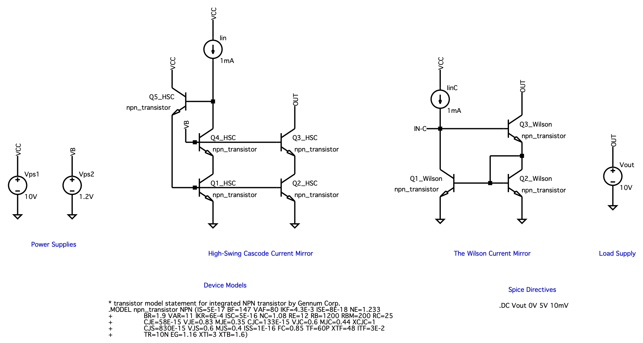
Fig. 6.21: A high-swing cascode current mirror circuit with base-current compensation. Various voltage sources are used to separately monitor different branch currents.
|
|
|
|
Fig. 6.22: The circuit schematic for the high-swing cascode-current mirror and Wilson current mirror circuits captured in LTSpice for comparing iout-Vout behavior. |
|
|
|
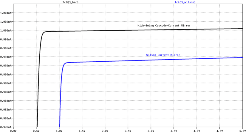
Fig. 6.23: Comparing the Iout -- Vout behavior of the high-swing cascode current mirror with that of the Wilson current mirror. Each transistor is modeled after a small npn integrated transistor manufactured by Gennum Corp.
|
6.5 A High-Performance Current Mirror
One means of decreasing the minimum output voltage of a current mirror circuit whose output is derived from the transistor action of two transistors stacked one above the other is to reduce the voltage that appears at the base of the top transistor. In this way, the voltage that can appear at the output of the current mirror can be reduced without the top transistor saturating. The circuit shown in Fig. 6.21 accomplishes this task while maintaining the high output resistance through the cascode output. Here the voltage at the base of Q3 and Q4 is set by the external voltage source VB. Correspondingly, the voltage at their respective emitters is one diode drop lower at about (VB - 0.7) V. Clearly, then, if VB is set between 1.0 V and 1.4 V, then the voltage at the emitter of Q3 will fall somewhere between 0.3 V and 0.7 V. Thus, the voltage at the output terminal of the current mirror can be reduced to about 0.6 - 1.0 V before Q3 saturates (assuming Q3 saturates at 300 mV). The other nodes in the circuit are set at levels that ensure that the other transistors are operating in their active regions. Transistor Q5 is used to compensate for the base current of Q1 and Q2.
We shall now compare the behavior of this high-swing cascode-current mirror circuit shown in Fig. 6.21 with the Wilson current mirror circuit shown in Fig. 6.13(c). The input to the current mirror will be set to 1 mA. The LTSpice circuit schematic capture for the high-swing cascode-circuit together with the Wilson current mirror is shown in Fig. 6.22. A DC sweep of the output voltage beginning at 0 V and increased +5 V in increments of 10 mV is requested. The collector current from transistor Q3 will then be plotted as a function of the output voltage. The transistor is modeled using the Gennum Corporation IC transistor model described earlier.
The results of the LTSpice analysis are shown plotted in Fig. 6.23. As can be seen, the output current from the high-swing cascode-current mirror is much closer to the input current of 1 mA than in the case of the Wilson current mirror, i.e., the new circuit behaves in a more ideal fashion. Although it is not readily apparent, the high-swing cascode current-mirror has an output resistance about twice that of the Wilson current mirror of about 6.5 MΩ. This output resistance value was determined with the aid of the cursor facility of the waveform viewer. With regards to the minimum output voltage, we see that the high-swing cascode mirror circuit does indeed succeed at its primary objective of reducing the minimum output voltage below that of the Wilson current mirror, specifically it can operate with a voltage as low as 0.7 V.
|
Fig. 6.24: A simple current-mirror circuit setup as a current source.
Fig. 6.25: The circuit schematic for the current source arrangement captured in LTSpice for investigating iout-Vout behavior. |
|
Fig. 6.26: Iout vs. Vout for the current source implementation shown in Fig. 6.24.
|
Fig. 6.27: Norton equivalent representation of the current source in Fig. 6.24 for Vout > 220 mV.
|
6.6 Current-Source Biasing in Integrated Circuits
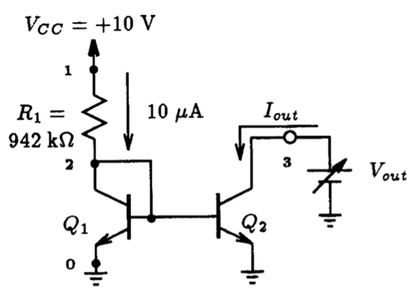
A typical approach for implementing a current source in IC technology is with current mirror circuits. Figure 6.24 illustrates a simple current mirror arranged as a current source. The input terminal of the current mirror is fed with a 942 kΩ resistor connected to the positive power supply. This results in an input bias current of about 10 𝜇A. The output terminal is connected to a variable DC voltage source Vout to simulate the action of a load. With the aid of LTSpice, we would like to determine the range of output voltages that can appear across the output port of the current mirror before the circuit ceases to operate as a current source. In addition, we would also like to determine the Norton equivalent circuit representation of the output port of this current mirror. We shall assume that the transistors are matched and are typical of the small npn integrated transistor variety manufactured by the Gennum Corporation. As mentioned before, these transistors have a forward βac of approximately 90 at a bias current of 1 mA and an Early voltage in the neighborhood of 80 V.
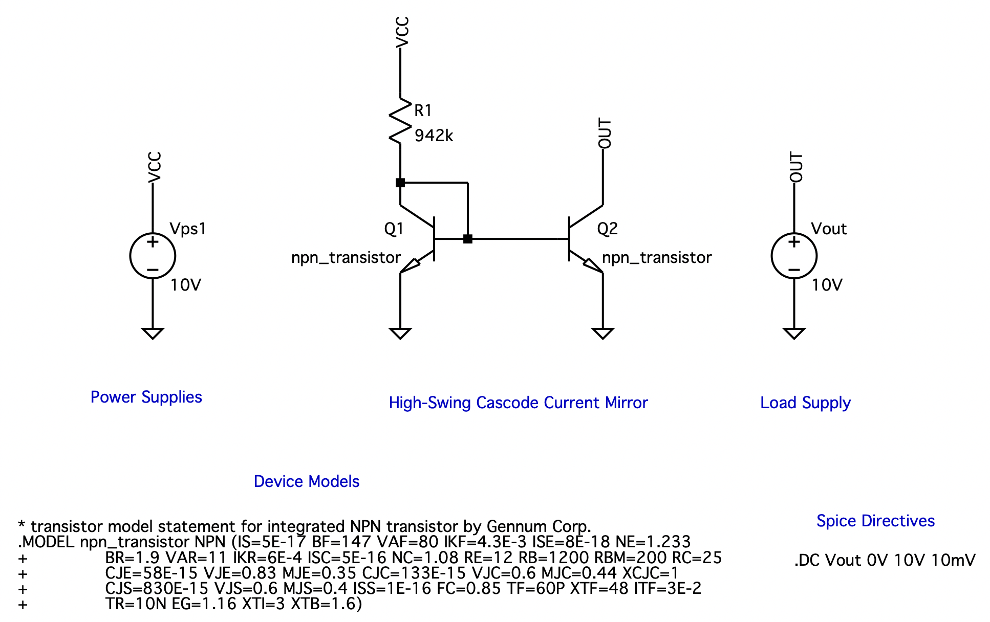
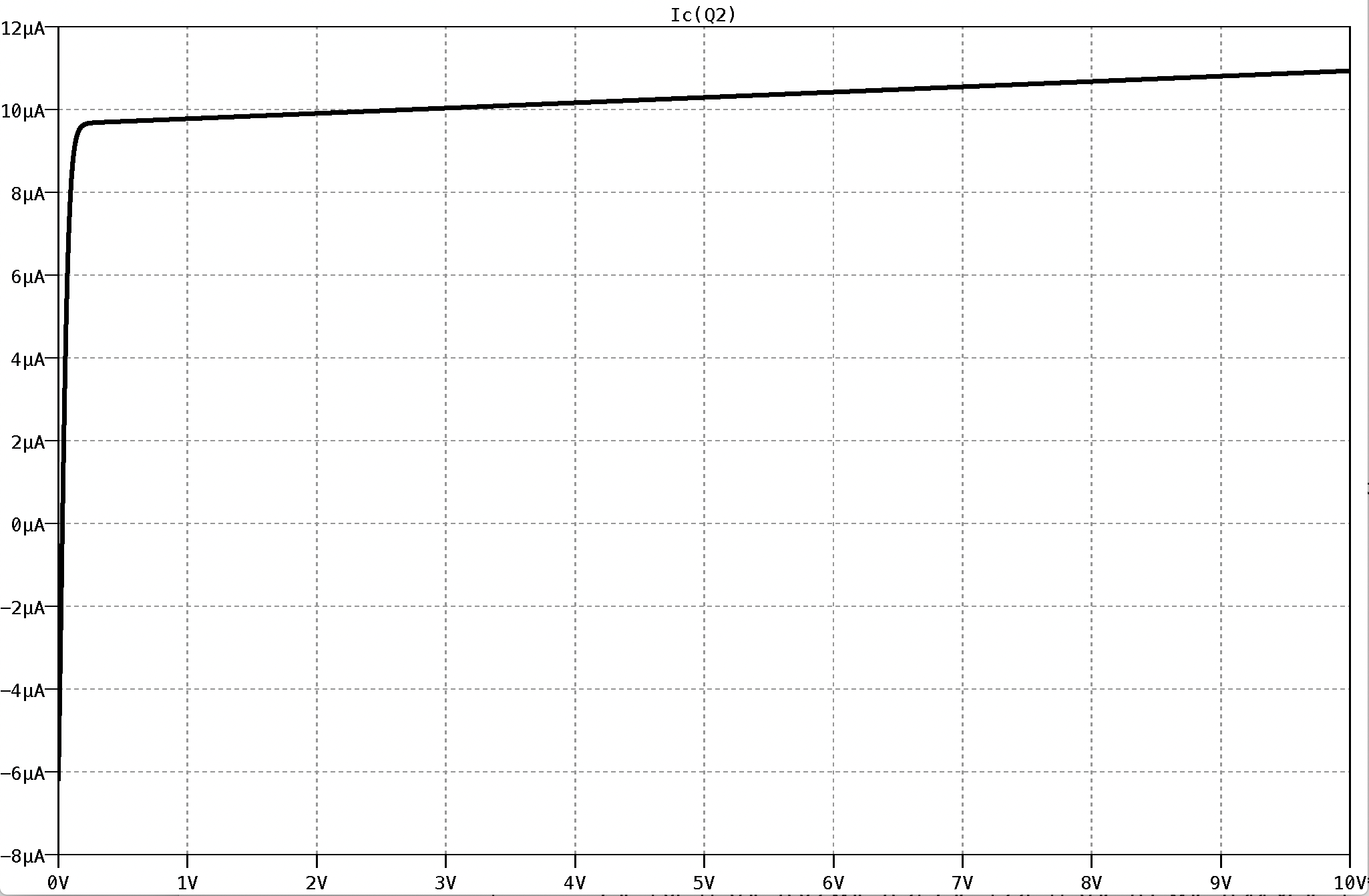
The LTSpice schematic captured describing this circuit is shown in Fig. 6.25 where we have requested a DC sweep of the output voltage Vout beginning at 0 V and ending at 10 V. The output collector current of Q2 will then be plotted as a function of Vout. The results of the LTSpice analysis are shown in Fig. 6.26. For output voltages larger than 220 mV, we see that the output current remains relatively constant around 10 𝜇A, increasing slightly at a rate of 0.13 𝜇A per volt. When the output voltage drops below 220 mV the output current drops quickly to zero amps. Thus, the circuit operates as an effective current source provided the voltage appearing across the output remains above 220 mV.
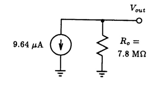
We can go further and characterize the output port of this circuit (assuming Vout > 220 mV) using the Norton equivalent circuit as shown in Fig. 6.27. The level of the current source of 9.64 𝜇A was found by finding the y-axis intersection of the extrapolated line joining the points on the i-v curve in Fig. 6.24 for Vout > 220 mV. The output resistance Ro=7.8 MΩ is simply the inverse of the slope of this line found using the cursor facility of the waveform viewer. It is interesting to note that a similar resistance value is found through a .TF command with the output voltage biased somewhere inside the linear region of the current source.
It is also reassuring that hand analysis also generates a value of the output resistance for the current source that is in the neighborhood of that predicted by LTSpice, i.e., VA / I = 80 V / 10 𝜇A = 8 MΩ. The effect of the emitter resistance of 12 Ω is not very significant at a current level of 10 𝜇A because the transistor transconductance is small, i.e., 0.4 mA/V. Thus, from Eqn. (6.1}, we see that Ro does not change by much, e.g., Ro » [ 1 + (0.4 x 10⁻³)(12)](8 x 106) = 8.04 MΩ.
|
Fig. 6.28: A CMOS differential pair with active load and current source biasing.
Fig. 6.29: The circuit schematic for CMOS differential pair with active load and current source biasing captured in LTSpice. |
|
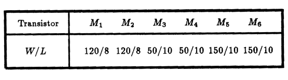
Table 6.3: Transistor dimensions of the CMOS amplifier in Fig. 6.25.
|
|
Fig. 6.30: The large-signal differential-input transfer characteristics of the CMOS amplifier shown in Fig. 6.28.
|
Fig. 6. 31: An expanded view of the high-gain differential region of the CMOS amplifier shown in Fig. 6.28.
|
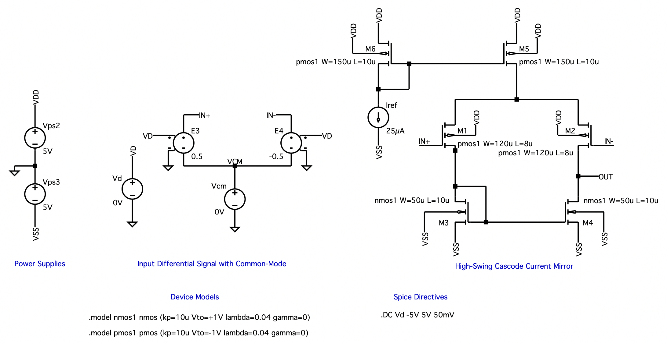
6.7 A CMOS Differential Amplifier with Active Load
Differential pairs, current mirrors and current sources are usually combined in MOS technology to form differential amplifiers. The current source is used to bias the differential pair and the current mirror acts as a large resistive load, thus providing large voltage gain. An example of a CMOS differential amplifier is shown in Fig. 6.28. It is easily shown by hand analysis that the small-signal differential-mode voltage gain Ad of this stage is given approximately by Ad=- gm1 (ro2 || ro4). The corresponding common-mode voltage gain ACM is, to a first order approximation, zero. An expression for ACM can be derived through a small-signal analysis, however, the result is usually too complex to be insightful.
Using LTSpice let us compute the differential-mode and common-mode voltage gains of the differential amplifier shown in Fig. 6.28, and thus, its common-mode rejection ratio (CMRR). We shall assume that the NMOS and PMOS transistors are fabricated with a CMOS process which can be characterized by the following Spice model parameters: 𝜇nCOX=20 𝜇A/V2, 𝜇pCOX=10 𝜇A/V2, |Vt|=1 V, and 𝜆=0.04 V-1. For the time being we shall neglect the body effect of the transistor (i.e., 𝛾=0). The length and width dimension of each transistor are listed in Table 6.3.
The LTSpice schematic capture with Spice directive can be seen in Fig. 6.26. The input is excited using the multiple-source arrangement depicted in Fig. 6.3. The first analysis that is requested is a DC sweep of the input differential voltage. The input differential voltage is swept between the two voltage supply limits (i.e., -5 V and +5 V) with a voltage increment of 50 mV. This LTSpice analysis will then be followed by a DC sweep of the input common-mode voltage. These two DC sweeps are necessary to locate the high-gain linear region of the amplifier.
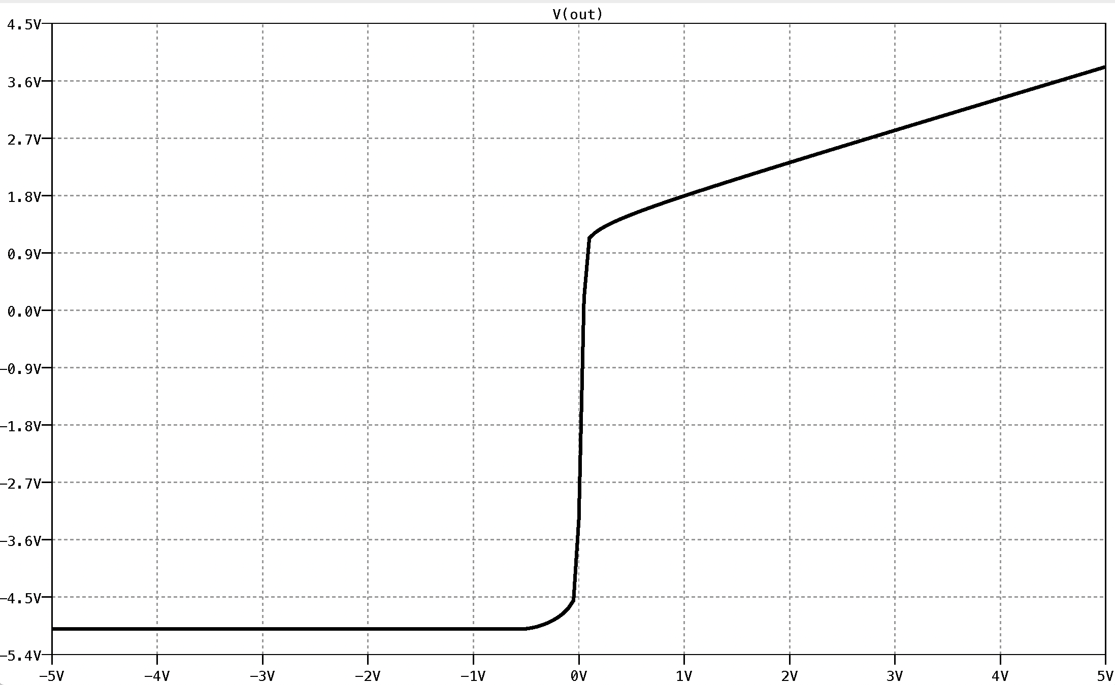
The large-signal differential-input transfer characteristic of the CMOS amplifier as calculated by LTSpice is shown in Fig. 6.30. Here we see that the high-gain region is in the vicinity of 0 V. However, pertinent details of this region are not clearly evident. We shall therefore re-run the LTSpice analysis using a more refined step size for Vd. Specifically, we shall replace the DC sweep command given earlier by the following one:
.DC Vd -100mV +100mV 1mV
On completion of the LTSpice, we observe the expanded view of the CMOS amplifier high-gain region in Fig. 6.31. As is evident, this particular amplifier has an output DC offset of -3.5 V, or equivalently an input offset voltage of -50 mV. The linear region of this amplifier is between Vd=-10 mV and +65 mV. To obtain the small-signal differential gain in this region we can either estimate it from the slope of the line forming the amplifier linear region, or calculate it directly using a .TF command. We shall choose the latter and enter the following .TF command in the LTSpice schematic seen in Fig. 6.29:
.TF V(OUT) Vd
Most applications of differential amplifiers involve using them in a negative feedback configuration where the negative feedback forces the input differential voltage towards zero. It seems reasonable, therefore, to evaluate the differential gain and other characteristics with the transfer characteristics shifted so that the input referred offset voltage is zero. This can be achieved by applying a differential offset voltage of +50 mV to the input of the amplifier, i.e., modify the Vd source attributes to have a value of 50 mV. The result of the LTSpice analysis is as follows:
The small-signal differential gain Ad is therefore 67.43 V/V. To compare this quantity with that estimated by hand, we recall that Ad=- gm1 (ro2||ro4) and
![]()
Thus, we can estimate gm1 to be 86.6 mA/V by assuming ID1=12.5 𝜇A. Similarly, the output resistance of M2 and M4 is given by ro= 1/𝜆 ID = 1 /(0.04 * 12.5 x 10-6) which gives ro=2 MΩ. Substituting these values into the expression for Ad results in Ad=86.6 V/V. When compared to the gain computed by LTSpice, our estimate here has a relative error of about 28%. The reason for this error is largely due to the inaccuracy in estimating the drain bias current of each transistor, which in turn is the result of neglecting the Early effect.
A better estimate of the differential voltage gain can be obtained by using the bias point and thus the small-signal model parameters generated by LTSpice. These are listed below on completion of a .OP analysis:
|
Semiconductor Device Operating Points:
--- MOSFET Transistors --- Name: m6 m5 m2 m1 m3 Model: pmos1 pmos1 pmos1 pmos1 nmos1 Id: 2.50e-05 2.69e-05 1.43e-05 1.26e-05 1.26e-05 Vgs: 0.00e+00 2.04e+00 -2.26e-01 3.34e+00 1.69e+00 Vds: 1.56e+00 3.60e+00 1.20e+00 4.71e+00 1.69e+00 Vbs: 1.56e+00 3.60e+00 4.80e+00 8.31e+00 0.00e+00 Vth: -1.00e+00 -1.00e+00 -1.00e+00 -1.00e+00 1.00e+00 Vdsat: -5.60e-01 -5.60e-01 -4.26e-01 -3.76e-01 6.88e-01 Gm: 8.93e-05 9.61e-05 6.70e-05 6.71e-05 3.67e-05 Gds: 9.41e-07 9.41e-07 5.45e-07 4.25e-07 4.73e-07 Gmb: 0.00e+00 0.00e+00 0.00e+00 0.00e+00 0.00e+00
|
Using these, we compute the differential voltage gain Ad to be 66.4 V/V. This is obviously much closer to the value computed by LTSpice at 67.43 V/V. Once again, we see that the small-signal gain expression derived by hand result in accurate gain prediction provided that good estimates of the bias points and hence of the small-signal model parameters of the transistors are used.
|
|
|
Fig. 6.32: The large-signal common-mode DC transfer characteristics of the CMOS differential amplifier shown in Fig. 6.28. An input differential offset voltage of +50 mV is applied to the amplifier input to ensure that the amplifier is biased in its linear region.
|
In a similar fashion, the large-signal common-mode transfer characteristic of the amplifier is computed by replacing the DC sweep command in the LTSpice schematic window seen in Fig. 6.29 by one that sweeps the input common-mode voltage (VCM) between -5 V and +5 V in 50 mV increments. The syntax of such a Spice directive would appear as follows:
.DC Vcm -5V +5V 50mV.
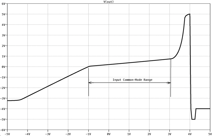
The revised LTSpice schematic is then re-run and the effect of the input common-mode signal level on the output is plotted in Fig. 6.32. Here we see that an input common-mode level ranging between -1 V and +3 V has little effect on the output signal. For instance, a 1 V change in the input common-mode level causes a +180 mV change in the output voltage level and this is fairly consistent over the -1 V to +3 V range. In other words, the common-mode gain ACM is approximately 180 mV/V. This also can be confirmed by using a .TF command. However, the estimate we obtained directly from the transfer characteristic shown in Fig. 6.32 is sufficiently accurate for our purposes here.
We should note here that once the common-mode range is known we must check to see whether the VCM used to determine the large-signal differential characteristic is valid. Specifically, the large-signal differential characteristic computed earlier was obtained with VCM=0 V. Fortunately, this lies within the common-mode range of the amplifier, and the differential characteristics obtained are therefore valid.
Combining the above estimate of the amplifier common-mode gain with the small-signal differential gain calculated earlier, we can compute the CMRR of the amplifier to be 66.4/180 x 10-3=368.9 or 51.3 dB.
In the above analysis we ignored the presence of transistor body effect (i.e., 𝛾=0). In the following we shall repeat the above analysis with 𝛾=0.9 V1/2. This requires that we alter the two MOS model statement provided in the LTSpice circuit schematic seen listed in Fig. 6.26 according to:
.model pmos_transistor pmos (kp=10u Vto=-1V lambda=0.04 gamma=0.9 )
.model nmos_transistor nmos (kp=20u Vto=+1V lambda=0.04 gamma=0.9 )
Repeating each Spice analysis suggested above, we then find the following differential-mode and common-mode voltage gains of 70.77 V/V and 139.2mV/V, respectively. Comparing these results with those computed without the body effect taken into account, we see that both Ad and ACM have changed a little. The new CMRR then becomes 54.1 dB; an increase of 2.8 dB.
|
Fig. 6.33: A simple MESFET differential amplifier.
Fig. 6.34: The circuit schematic for the simple MESFET differential amplifier captured in LTSpice. Here five Spice directives will be used to characterize the amplifier. |
|
|
|
|
Fig. 6.35: The large-signal differential DC transfer characteristics of the MESFET differential amplifier shown in Fig. 6.33 with VCM=0V.
|
Fig. 6.36: An expanded view of the linear region of the differential DC transfer characteristics of the MESFET differential amplifier shown in Fig. 6.33 with VCM=0 V.
|
6.8 GaAs Differential Amplifiers
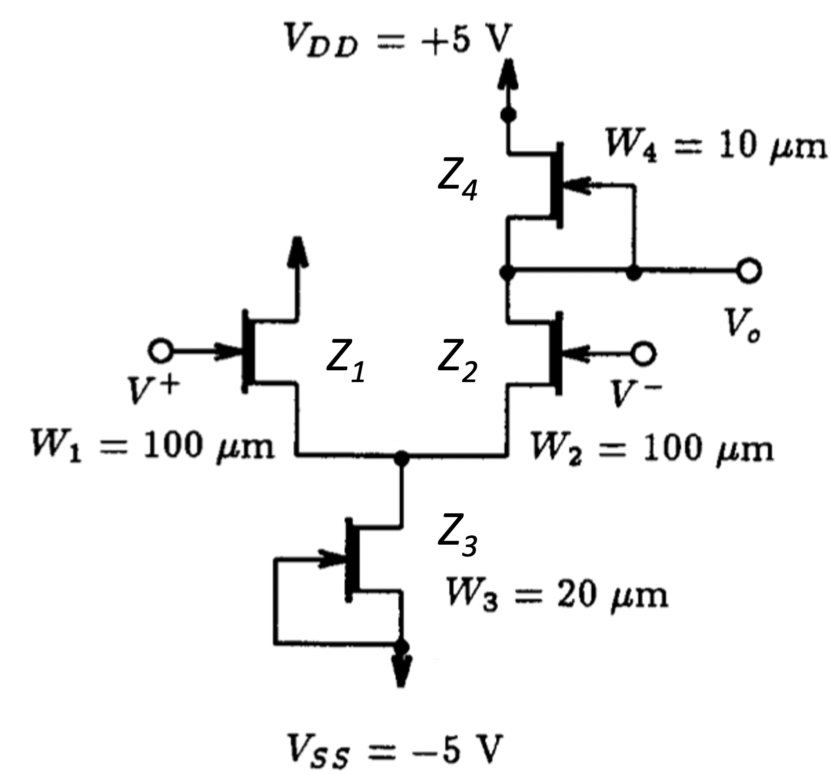
In Fig. 6.33 we show a simple GaAs MESFET differential amplifier. Each MESFET is assumed to have minimum length (1 um in this case), but their widths vary and are specified alongside each transistor. Using LTSpice we would like to compute the large-signal differential and common-mode DC transfer characteristics of this amplifier. From this, we would like to determine its common-mode rejection ratio (CMRR). We shall assume that the MESFETs are characterized by the following parameters: β=0.1 mA/V2 (for a 1-um wide device), Vt=-1.0 V, and 𝜆=0.05 V-1.
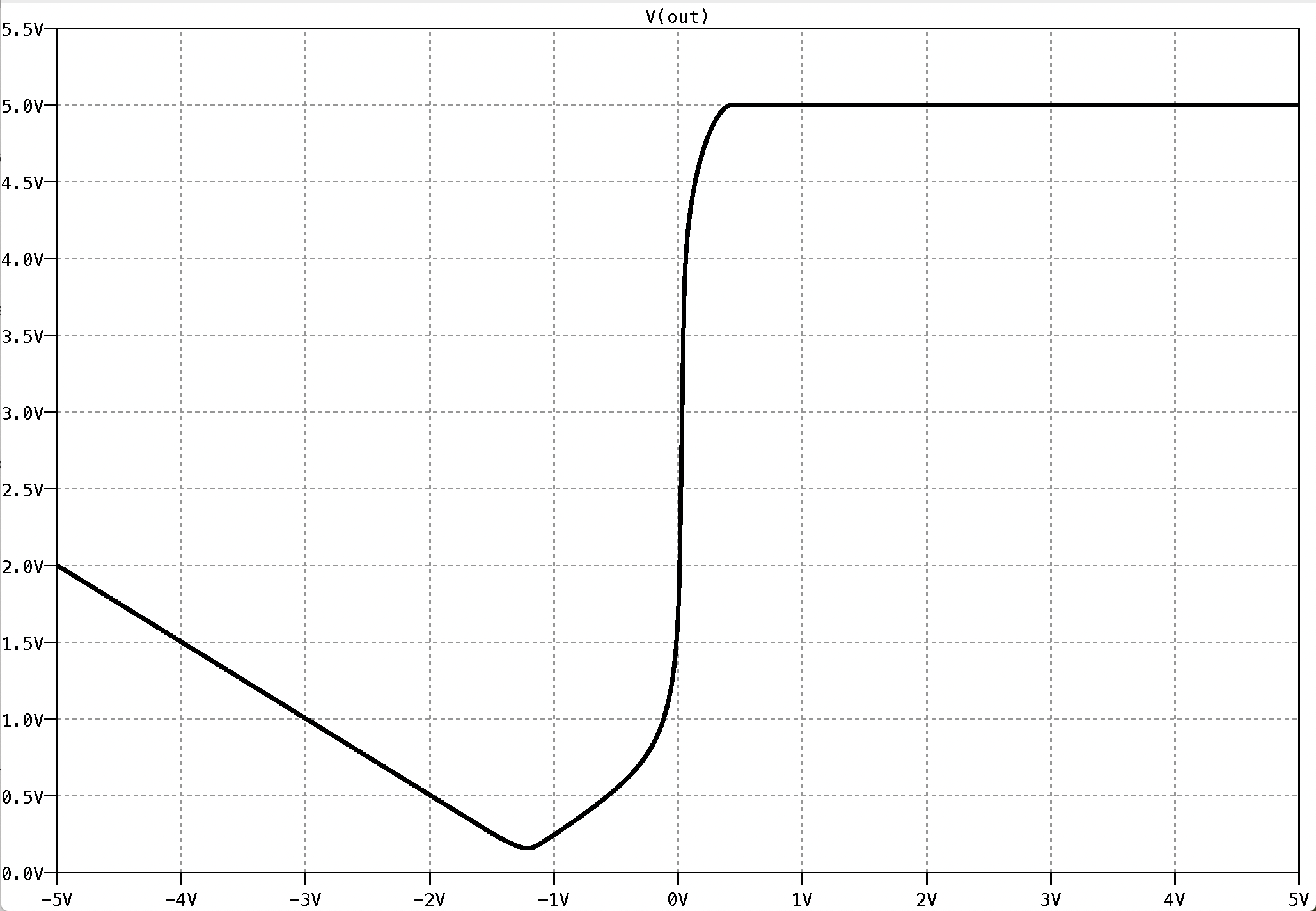
The LTSpice schematic capture of the circuit of Fig. 6.33 is shown in Fig. 6.34. The inputs to this amplifier are assumed to be driven by the same multiple voltage source combination shown connected to the input terminals of the circuit in Fig. 6.3. To obtain the large-signal DC differential transfer characteristic we shall perform a DC sweep of the input differential voltage between the voltage limits of the two supplies (i.e., VDD=+5 V and VSS=-5 V) using a 10-mV step. The input common-mode level VCM shall be set equal to zero, as it is usually assumed that VCM=0 V is an input that will be within the linear range of the amplifier.
On completion of the LTSpice analysis the large-signal differential characteristic shown in Fig. 6.35 is found. Here we see a rather strange large-signal differential transfer characteristic. Instead of the output voltage swinging between the limits of the two power supplies, the output only swings between VDD and ground - about one-half the normal voltage swing. We also notice that below the high-gain region of the amplifier, for input levels less than -1 V, the output level does not saturate, but instead begins to rise in a very linear manner. This suggests that this amplifier has a limited range of operation as a differential amplifier and therefore the input differential voltages must be restricted to be greater than -1 V.
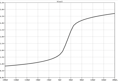
To obtain a better view of the linear region of this amplifier, we shall re-sweep the input differential voltage between -200 mV and +200 mV using a step size of 10 mV. This requires that we alter the DC sweep command in the LTSpice command window of Fig. 6.34 to the following one:
.DC Vd -200mV +200mV 10mV.
Re-running the LTSpice analysis, we obtain the large-signal characteristic of the amplifier shown in Fig. 6.36. We see that the slope of the linear region is rather low, approximately 50 V/V, extending between 10 mV and 50 mV along the Vd axis. Such low voltage gain can be attributed to the rather low channel-length modulation factor of the MESFET (i.e., 𝜆=0.05 V-1). As an estimate of the small-signal voltage gain in the high gain region of this amplifier, consider evaluating the small-signal transfer characteristic of this amplifier using the .TF command around an input differential voltage of 30 mV. This point was chosen because it lies approximately midway between the two extremes of the linear region. The following .TF command is placed in the LTSpice command window shown in Fig. 6.34,
.TF V(OUT) Vd.
and the attributes of the input differential voltage Vd is modified to include the input 30 mV offset voltage according to
Vd VD 0 DC 30mV.
On completion of this analysis, the transfer function gain is found to be 51.8 V/V. This low gain can be attributed to the rather low output resistance of the amplifier (i.e., Ro=12.38 kΩ).
According to a hand analysis the voltage gain and output resistance of the differential amplifier shown in Fig. 6.33 are given by Ad=gm2Ro and Ro=(ro2||ro4). To check these expressions against the values computed by LTSpice, we list below the parameters of the small-signal model of each MESFET as computed by LTSpice:
|
Semiconductor Device Operating Points:
--- MESFETS --- Name: z1 z2 z4 z3 Model: n_mesfet n_mesfet n_mesfet n_mesfet Id: 1.13e-03 8.51e-04 8.51e-04 1.98e-03 Vgs: -6.81e-01 -7.11e-01 0.00e+00 0.00e+00 Vds: 4.30e+00 2.19e+00 2.12e+00 5.70e+00 Gm: 6.76e-03 5.66e-03 1.50e-03 3.50e-03 Gds: 4.63e-05 3.83e-05 3.85e-05 7.69e-05 Cgs: 0.00e+00 0.00e+00 0.00e+00 0.00e+00 Cgd: 0.00e+00 0.00e+00 0.00e+00 0.00e+00
|
Substituting the appropriate parameter values into the expression for Ro and Ad above, we get Ro=13 kΩ and Ad=73.6 V/V. When comparing these with those generated by LTSpice (i.e., Ro=12.38 kΩ and Ad=45.4 V/V), we see that our small-signal hand calculations are not as accurate as we've seen previously for Bipolar and CMOS technologies. The reason for this is that the large-signal model used to describe the small-signal operation of the MESFET is different than that used by LTSpice. As a result, the small-signal models are slightly different. This was not the case for the other technologies. Here it should be noted that the development of accurate GaAs MESFET models is still a subject of current research.
|
|
|
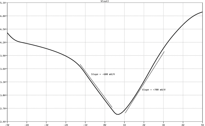
Fig. 6.37: The large-signal common-mode DC transfer characteristics of the MESFET differential amplifier shown in Fig. 6.30. The input differential offset voltage is set equal to 25 mV.
|
|
|
|
|
|
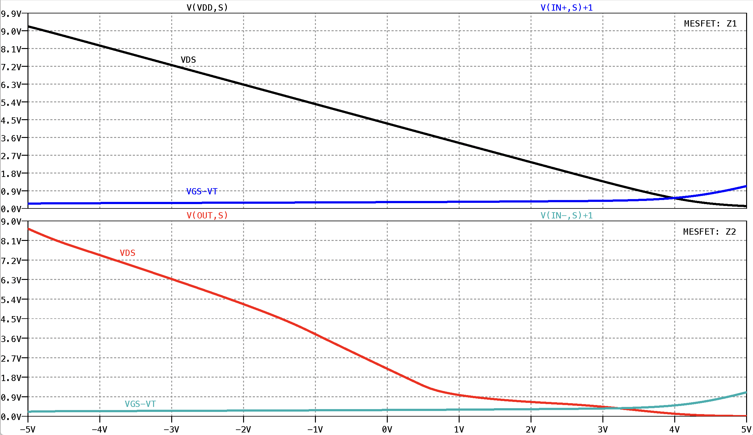
Fig. 6.38: Investigating the mode of operation of each MESFET in the amplifier of Fig. 6.33. Here we are comparing VDS with VGS - Vt of each MESFET and determining the range of input common-mode voltage that maintains each transistor in its linear region.
|
||
To determine the large-signal DC common-mode transfer characteristics of the MESFET amplifier in Fig. 6.33 we require that LTSpice compute the output voltage as a function of the input common-mode voltage. This is easily achieved by modifying the Spice directive seen listed in Fig. 6.34 by replacing the DC sweep command given there by the following one:
.DC Vcm -5V +5V 100mV.
The input differential voltage Vd will remain offset by 30 mV in order to keep the amplifier in its linear region.
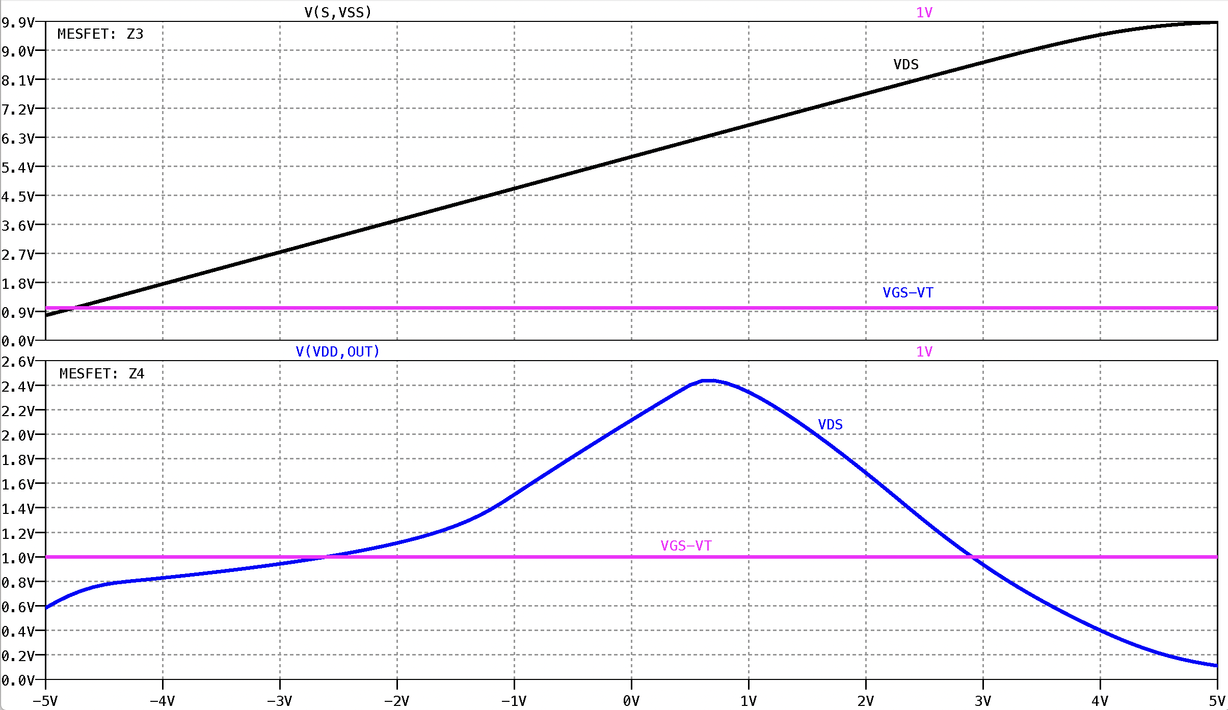
Re-submitting this revised command to LTSpice results in the large-signal common-mode transfer characteristic shown in Fig. 6.37. Here we see that the common-mode characteristic consists of two almost linear regions with opposite signed slopes. For input common-mode voltages less than 0.66 V, the slope of the large-signal characteristic is negative with a magnitude estimated directly from the graph to be approximately -600 mV/V. Whereas, for input common-mode voltages larger than 0.66 V, the slope is estimated to be about +700 mV/V. This rather unusual looking characteristic is a result of the low output resistance of MESFETs.
The input common-mode range of this amplifier is not obvious from the graph of the output voltage as a function of the input common-mode voltage. But it can be determined by plotting the drain-source voltage VDS of each MESFET as a function of the input common-mode voltage and compare it to the corresponding gate-source voltage minus the threshold voltage VGS-Vt of each MESFET. If VDS ³ VGS - Vt, then the MESFET is in its linear region, otherwise it is not. The same LTSpice circuit capture can be used here without any modifications. Recall that Vt is equal to -1 V. The results, as further calculated and displayed by the waveform viewer, are shown in Fig. 6.38. From these results we see that the upper linear region of this amplifier is determined by MESFET Z2 entering the triode region for VCM exceeding +3 V. The lower common-mode input range limit is determined solely by Z3: When the VCM decreases below -4.7 V, this transistor enters triode. Therefore, the common-mode input range (CMR) for this amplifier is between -4.7 and +3 V. We note that a common-mode input voltage of 0 V is within the CMR of this amplifier and thus our previous calculation of differential-mode gain is valid.
To estimate the CMRR of this amplifier, we have to consider that when the input common-mode voltage is less than 0.66 V, the common-mode gain ACM is about -600 mV/V and when the input common-mode voltage is greater than this amount, ACM=+700 mV/V. Thus, using the worst-case situation, that is, when |ACM| is largest, the CMRR is computed according to 20log(|Ad|/|ACM|) = 20 log (51.8 V/V / 0.7 V/V ) to be 37.4 dB.
|
Fig. 6.39: A simple multi-stage operational amplifier consisting of 3 stages.
Fig. 6.40: The circuit schematic for the three-stage operational amplifier captured in LTSpice. Here five Spice directives are used to characterize the amplifier. |

|
Fig. 6.41: The large-signal differential transfer characteristic of the operational amplifier shown in Fig. 6.36. The input common-mode voltage VCM is set to zero.
|
Fig. 6.42: An expanded view of the high-gain differential region of the operational amplifier shown in Fig.6.39.
|
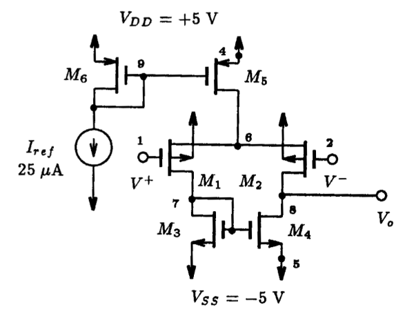
6.9 A BJT Multistage Amplifier Circuit
Fig. 6.39 illustrates the circuit of a simple operational amplifier. It consists of a cascade of several gain stages, two of which are made from differential pairs, and an output buffer. The positive and negative input terminals to the amplifier are labeled as V+ and V-, respectively. The output terminal is denoted as Vo. For the purpose of our analysis we shall assume that both the npn and pnp transistors have the following device parameters: IS=18 fA, βF=100, VAF=100 V. In addition, Q6 is considered to have 4x the area of Q9 and Q3. This is achieved by appending to the model name call the area multiplier factor. In this case, the number 4 is included. Using LTSpice, we would like to analyze this operational amplifier to determine its DC operating point which includes such information as output offset voltage, input bias currents and quiescent power dissipation. In addition, we would also like to compute the small-signal differential voltage gain (in the high gain region of the amplifier) and the input common-mode range.
The schematic captured with LTSpice for the operational amplifier, together with the multiple input voltage source arrangement discussed in section 6.1, is shown in Fig. 6.40. Notice how Q6 is specified to have 4x the area of Q3 and Q9. Two analysis request commands are listed here: a DC operating point command and a DC sweep command. The .OP command is made active first.
The DC operating point command will, in addition to calculating the DC operating point of the circuit and the small-signal model parameters of each transistor, determine the input bias currents. The DC sweep command will be used to compute the large signal transfer characteristic of the amplifier by varying the DC level of the input differential source Vd between -15 V and +15 V in 100 mV increments. The common-mode input VCM will be held at zero volts throughout this DC sweep. One may be tempted to add a small-signal transfer function analysis request here; however, this should be deferred until one sees the large signal differential transfer characteristic of the amplifier and can determine what DC input conditions are required so that Spice linearizes the amplifier around a known operating point.
Executing the dc analysis with LTSpice results in the following DC analysis output:
|
Operating Bias Point Solution:
V(out1+) 9.42948 voltage V(in+) 0 voltage V(e1) -0.603468 voltage V(out1-) 9.42948 voltage V(in-) 0 voltage V(vcc) 15 voltage V(vee) -15 voltage V(vcm) 0 voltage V(vd) 0 voltage V(b9) -14.3794 voltage V(e4) 8.78677 voltage V(out2) 11.6173 voltage V(out3) 2.74917 voltage V(out) 2.0675 voltage V(e7) 12.2593 voltage Ic(Q7) -0.00118076 device_current Ib(Q7) -1.08457e-05 device_current Ie(Q7) 0.0011916 device_current Ic(Q6) 0.00233679 device_current Ib(Q6) 1.89726e-05 device_current Ie(Q6) -0.00235576 device_current Ic(Q8) 0.00563893 device_current Ib(Q8) 5.02351e-05 device_current Ie(Q8) -0.00568917 device_current Ic(Q5) 0.00113841 device_current Ib(Q5) 1.11404e-05 device_current Ie(Q5) -0.00114955 device_current Ic(Q4) 0.0011761 device_current Ib(Q4) 1.11404e-05 device_current Ie(Q4) -0.00118724 device_current Ic(Q9) 0.000474316 device_current Ib(Q9) 4.74317e-06 device_current Ie(Q9) -0.00047906 device_current Ic(Q3) 0.000539658 device_current Ib(Q3) 4.74315e-06 device_current Ie(Q3) -0.000544401 device_current Ic(Q2) 0.000267385 device_current Ib(Q2) 2.44344e-06 device_current Ie(Q2) -0.000269829 device_current Ic(Q1) 0.000267385 device_current Ib(Q1) 2.44344e-06 device_current Ie(Q1) -0.000269829 device_current I(Rc6) 0.00568917 device_current I(Rc5) 0.00113052 device_current I(Rc3) 0.0011916 device_current I(Rc4) 0.00112757 device_current I(Rb) 0.000502775 device_current I(Rc2) 0.000278526 device_current I(Rc1) 0.000278526 device_current I(E2) -2.44344e-06 device_current I(E1) -2.44344e-06 device_current I(Vd) 0 device_current I(Vcm) -4.88688e-06 device_current I(Vps4) -0.0101989 device_current I(Vps3) -0.00969125 device_current
|
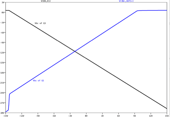
From these results, we see that this amplifier has an output DC offset of +2.0675 V and input bias currents of 2.443 𝜇A.
|
Table 6.4: DC collector currents of the operational amplifier shown in 6.36 expressed in mA as computed by hand analysis and LTSpice.
|
Table 6.5: Observing the variation in the DC collector currents (in mA) of the operational amplifier for different B's and VA's as computed by LTSpice. These can be compared with those computed by simple hand analysis. |
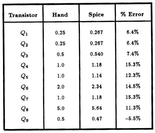
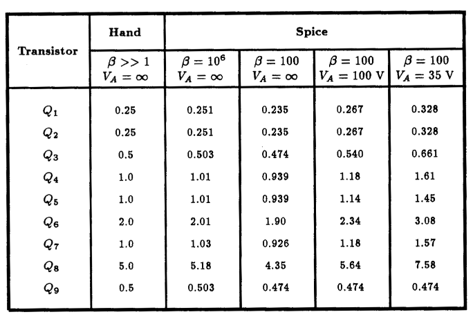
The collector currents of each device have also been computed by LTSpice; these have been arranged for easy access in Table 6.4. Also shown in this table are the currents computed by hand analysis, assuming that beta >> 1 and ignoring the effect of transistor Early voltage. A third column has also been added showing the relative error (in percent) between these two currents. As we can see, our hand estimates are reasonably close to the Spice results; the largest error in our estimates never exceeds 15.3%. It is reassuring that reasonably good estimates of the DC collector currents of a complicated transistor circuit can be obtained by assuming ideal transistor behavior (i.e., β >> 1 and VA=¥). As a further check on this, we compiled a table of collector current values that were computed by LTSpice for various combinations of β and VA values (IS remains at 18 fA) seen listed in Table 6.5. As one can see from this table, as beta and VA approach infinity (i.e., the transistors become more ideal), the results approach those computed by the simplified hand analysis.
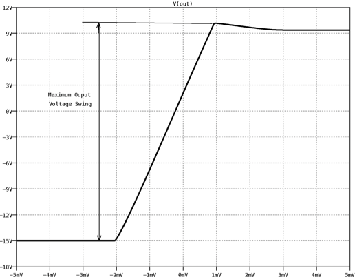
The large-signal differential transfer characteristic of this amplifier is displayed in Fig. 6.41 as derived by the activated .DC command and de-activated .OP command. This figure illustrates a view of the operational amplifier differential-input transfer characteristics between -15 V and +15 V. We recognize that the high-gain region of the amplifier is in the vicinity of 0 V; however, the resolution of the input voltage axis does not enable us to be certain of the boundaries of this high-gain region. Therefore, we shall re-run the LTSpice analysis with the DC sweep command modified to include an expanded view of this high-gain region between -5 mV and +5 mV. This will require that we replace the DC sweep command in the previous Spice input file with the following one:
.DC Vd -5mV +5mV 10uV
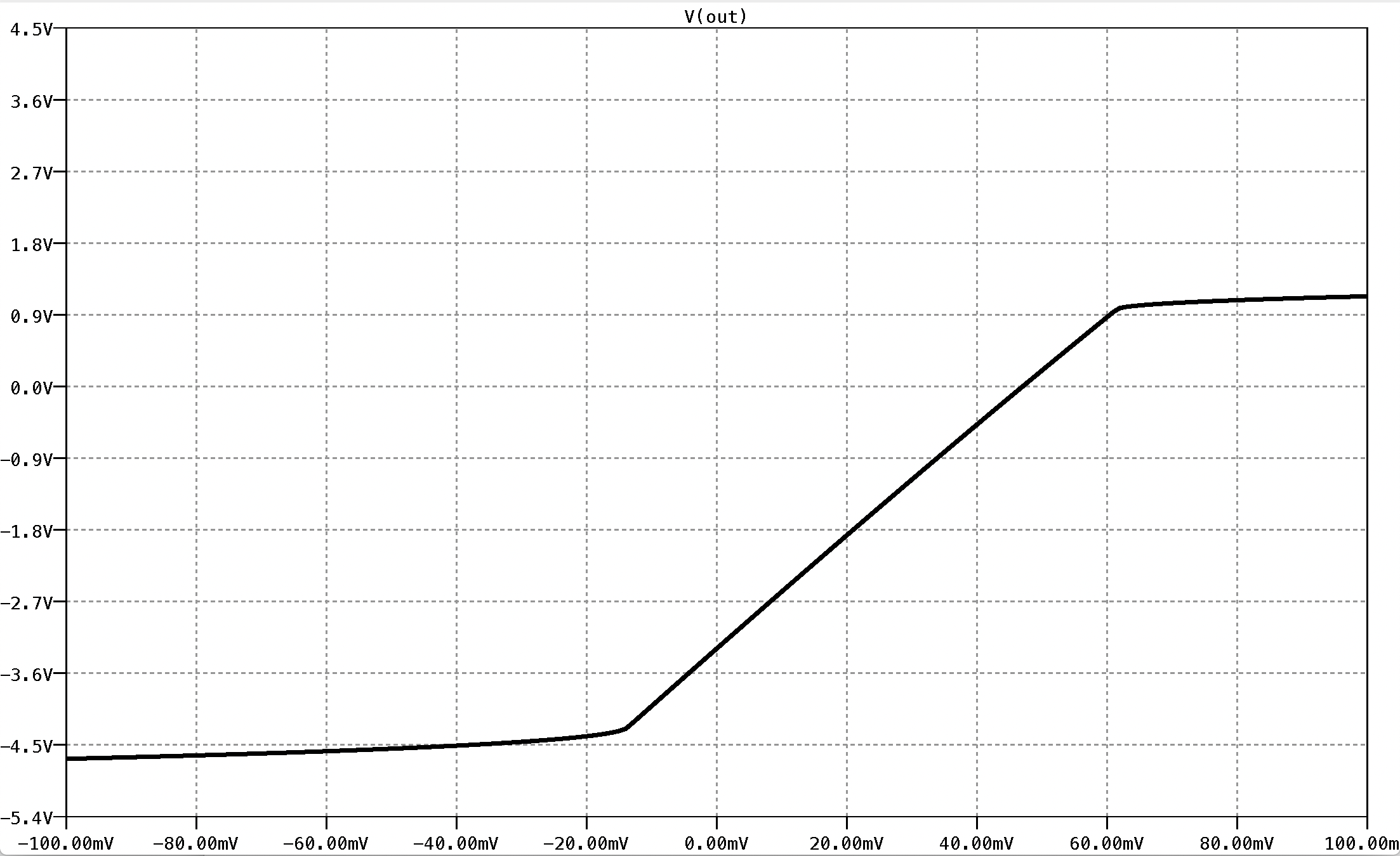
The results of this analysis are on display in Fig. 6.42. For inputs less than -2 mV, the output remains saturated at -15 V. In the region between -2 mV and +1 mV, the output level change from -15 V to +10 V in a linear manner. Thus, the output voltage swing for this amplifier is bounded between -15 V and +10 V, a somewhat unsymmetrical voltage swing. The gain experienced by input signals in this linear region is approximately (10 - (-15) )/3 mV = 8.33 kV/V. For inputs greater than +2 mV, the output levels' off at about 9 V. We also see from these results that the input offset voltage VOS for this amplifier is +230.0 𝜇V. This is of course the systematic offset of the amplifier and does not include the components due to various imbalances in the circuit (see Section 6.3).
Now that we know the boundaries of the high-gain region of the amplifier, we can use the transfer function command of LTSpice to compute the small-signal equivalent circuit parameters of the amplifier in its linear region. But first we must decide on which point inside the linear region of the amplifier we should linearize about. Consider that, for most applications, a high-gain amplifier such as that shown in Fig. 6.39 is usually used in conjunction with negative feedback, and, as a result, the output potential of the amplifier is held close to ground potential (when no input signal is applied). Thus, the small-signal parameters of the amplifier should be obtained around the bias point that has the amplifier output voltage close to 0 V. This is easily obtained by applying the negative of the amplifier input-referred offset voltage (i.e., -VOS) across the input terminals of the amplifier. For the multiple source arrangement suggested in Fig. 6.3, this is easily achieved by setting Vd equal to -VOS (in this case, -230 𝜇V).
Returning to the example at hand, we shall modify the attributes of the voltage source Vd to include an offset of -230 𝜇V, then run the following .TF directive,
.TF V(OUT) Vd
resulting in a small-signal differential gain of 8,834 V/V (found by plotting the result using the waveform viewer). This is very close to the value of 8,531 V/V that we extracted from the large-signal transfer characteristic of Fig. 6.42 using the cursor facility of the waveform viewer.
|
Fig. 6.43: The large-signal common-mode DC transfer characteristic of the BJT amplifier shown in Fig. 6.39. An input differential offset voltage of -230 𝜇V is applied to the amplifier input to prevent premature saturation.
|
Fig. 6.44: The effect of a common-mode input voltage VCM on the linearity of the input stage of the operational amplifier shown in Fig. 6.39. Here we illustrate the base-collector voltage of Q1 and Q3 as a function of VCM. The first stage of the amplifier leaves the active region when the base-collector junction of either Q1 or Q3 becomes forward bias. |
|
Table 6.6: Comparison of the results of the analysis of the operational amplifier shown in Fig. 6.36 by hand and using LTSpice.
|
The final analysis that we would like to perform on the operational amplifier shown in Fig. 6.39 is to determine its input common-mode range. Consider performing a DC sweep of the input common-mode voltage VCM between the rails of the two power supplies. This requires that we replace the DC sweep command stated in the Spice listing in Fig. 6.40 by the following one:
.DC Vcm -15V +15V 0.1V
We also maintain an input differential offset voltage of Vd = -230 𝜇V. This is necessary to ensure that the amplifier is biased inside its linear region.
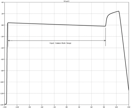
On execution, the amplifier’s large-signal common-mode transfer characteristic are displayed in Fig. 6.43. As we can see from these results, the transfer characteristic is linear behavior over the range of VCM between -14.2 V and +9.3 V. Outside these limits the characteristic becomes nonlinear. Thus, the input common-mode range for this amplifier is between -14.2 V and +9.3 V. We should also note that our large-signal differential transfer characteristic computed earlier is valid since it was obtained with an input common-mode voltage that falls within the input common-mode range of the amplifier.
It is interesting to correlate the limits of the amplifier common-mode range with the mode of operation of the transistors in the front-end stage. Specifically, the upper limit to the common-mode range is determined by Q1 or Q2 saturating, and that the lower limit is determined by Q3 saturating. We can determine when these transistors saturate by observing the voltage across the base-collector junction of each transistor and recalling that a transistor enters its saturation region when the base-collector junction becomes forward biased. For instance, in Fig. 6.44 we display the voltage across the base-collector junctions of Q1 and Q3 and observe that Q1 saturates when VCM exceeds +9.4 V. In contrast, transistor Q3 saturates when VCM goes below -14.3 V.
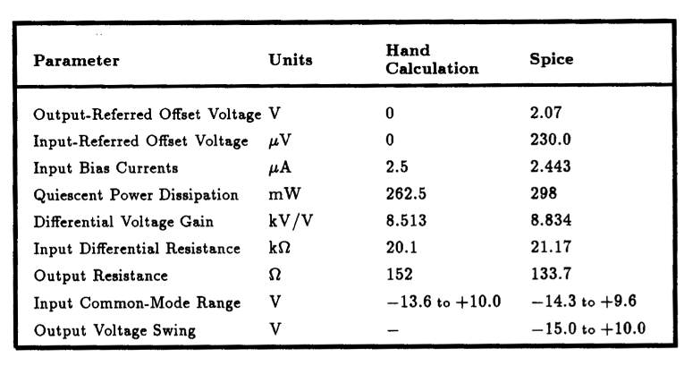
Finally, as a summary of what we have learned about this op-amp through the application of LTSpice, Table 6.6 presents a collection of the results. Moreover, these results are compared with the results of a simplified hand analysis.
6.10 Chapter Summary
· LTSpice can be conveniently used to compute both the large and small-signal characteristics of amplifier circuits.
· Inputs to differential amplifiers should consist of both a differential and common-mode level. An interesting arrangement of several voltage sources was given in this chapter (see Fig. 6.3, for instance), illustrating how the differential and common-mode levels can be independently adjusted.
· The high-gain linear region of an amplifier is located by first sweeping the input differential voltage vd between the limits of the power supplies with the common-mode voltage VCM equal to 0 V. This analysis is repeated with a reduced sweep range centered more closely around the high-gain region of the amplifier until a smooth transition through the high-gain region is achieved. Following this, one must check to see whether the input common-mode voltage of 0 V keeps the amplifier in its linear region.
· Care must be exercised when computing the small-signal characteristics of an amplifier using LTSpice. One should first decide what DC input conditions are required so that the amplifier is linearized around an appropriate DC operating point. Generally, selecting an input differential offset voltage that forces the output voltage to 0 V will bias the amplifier at an operating point that is quite close to the operating point that results when some external negative feedback connection is made around the amplifier.
· Any time an IC transistor is used in a circuit and its model is obtained from a library; the substrate connection must be defined.
· The small-signal input resistance to a differential amplifier is computed using LTSpice by applying a known AC voltage across the input terminals of the differential amplifier and computing the AC currents that flows into the amplifier terminals. In many practical amplifier situations, these currents will not be equal. So, instead, the average of these two currents is used in the input resistance calculation.
6.11 LTSpice Tips
· Random number generators are used to model a component whose value is treated as a random variable. There are three types of random number generator available in LTSpice: zero-mean value Gaussian distribution, zero-mean value uniform distribution, and a non-zero mean-value uniform distribution.
+ A zero-mean value Gaussian distributed random variable with standard deviation 𝜎 is called using the function gauss(𝜎).
+ A zero-mean value uniform distributed random variable from -𝜁 to 𝜁 is called using the function flat(𝜁).
+ A component with value 𝜇 that is uniformly distributed from 𝜇*(1-𝛿) to 𝜇*(1+𝛿) is called using the function mc(𝜇,𝜎).
+ All random variable calls must be placed inside brackets, { }.
· To invoke the selection of a new random component for a Spice analysis involving N trials, the following .STEP directive is used:
.STEP PARAM run 1 N 1
where run is just a dummy variable representing the sample iteration.
6.12 Bibliography
Staff,1990-1991 IC Data Book, Gennum Corporation, Burlington, Ontario, Canada.
6.13 Problems
6.1. A BJT differential amplifier is biased from a 2-mA constant-current source and includes a 100-Ω resistor in each emitter. The collectors are connected to +10 V via 5 kΩ resistors. A differential input signal of 0.1 V is applied between the two bases. Assume that the transistors are matched and have β=100 and IS=14 fA.
(a) With the aid of LTSpice, determine the signal current in the emitters ie and the base-emitter voltage vbe for each BJT.
(b) What is the total emitter current in each BJT?
(c) What is the signal voltage at each collector?
(d) What is the voltage gain realized when the output is taken between the two collectors?
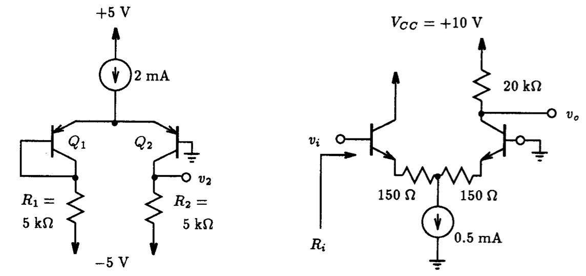
Fig. P6.2 Fig. P6.3
6.2. For the circuit in Fig. P6.2 in which the transistors have high β, with the aid of LTSpice, determine the value of v2. If the resistor R1 is reduced to 2.5 kΩ, what does v2 become?
6.3. Find the voltage gain and the input resistance of the amplifier in Fig. P6.3 using LTSpice assuming that β=100.
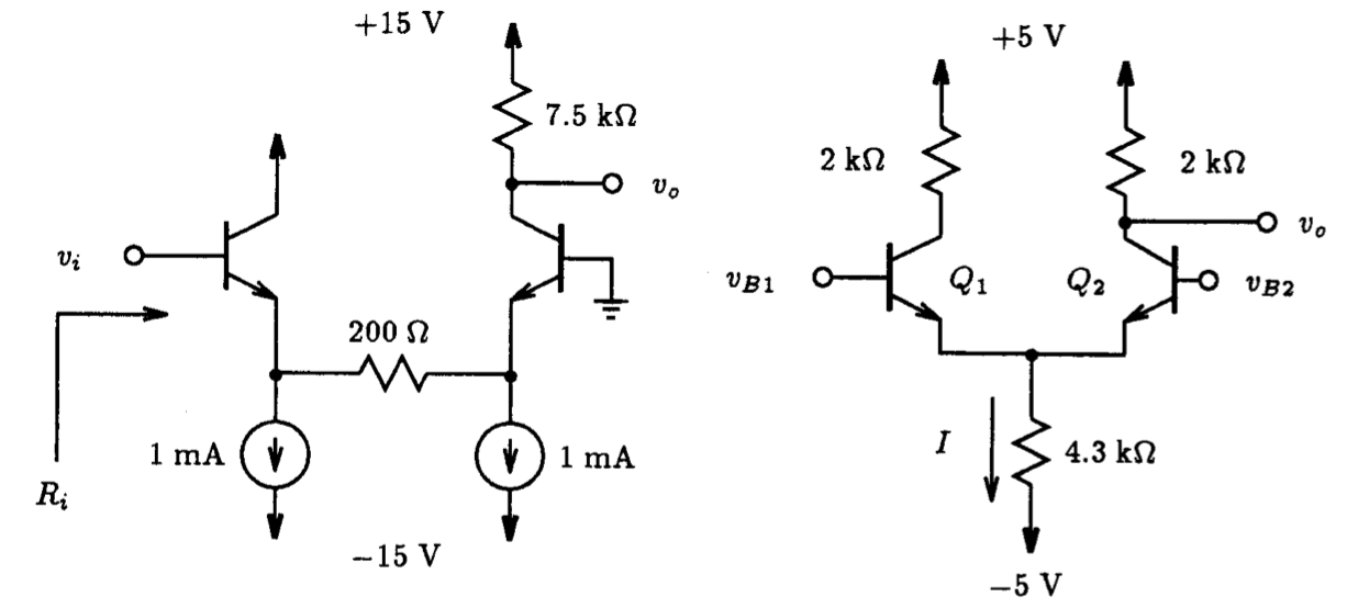
Fig. P6.4 Fig. P6.5
6.4. Find the voltage gain and the input resistance of the amplifier shown in Fig. P6.4 using LTSpice assuming β=100.
6.5. The differential amplifier circuit of Fig. P6.5 utilizes a resistor connected to the negative power supply to establish the bias current I.
(a) For vB1=vd/2 and vB2=-vd/2, where vd is a small signal with zero average, find the magnitude of the differential gain, |vo/vd| using LTSpice.
(b) For vB1=vB2=VCM, find the magnitude of the common-mode gain, |vo/VCM| using LTSpice.
(c) Calculate the CMRR.
(d) If vB1=0.1 sin(2p x 60t) + 0.005sin(2p x 1000t) volts, vB2=0.1sin(2p x 60t) - 0.005sin(2p x 1000t) volts, plot the output voltage vO using the waveform viewer of LTSpice.
6.6. A BJT differential amplifier is biased from a 300 𝜇A constant-current source and the collectors are connected to +7.5 V via 50 kΩ resistors. If the scale currents IS of the two transistors have a nominal value of 10 fA but differ by 10%, what is the resulting input offset voltage?
6.7. A BJT differential amplifier is biased from a 1 mA constant-current source and the collectors are connected to +15 V via a 10 kΩ resistors. If the β's of the two transistors are 100 and 200, what is the resulting input offset voltage?
6.8. A BJT differential amplifier is biased from a 1 mA constant-current source and the collectors are connected to +15 V via a 10 kΩ resistors. If VA of the two transistors are 100 and 200, what is the resulting input offset voltage?
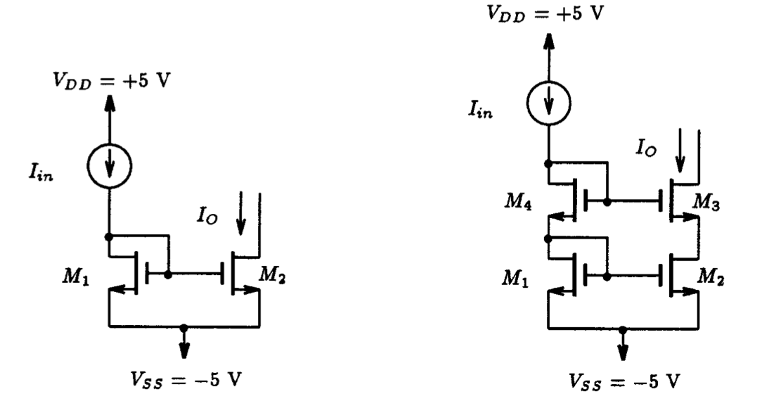
Fig. P6.9 Fig. P6.10
6.9. For the simple MOS current mirror shown in Fig. P6.9, the devices have Vt=1 V, 𝜇nCOX=200 𝜇A/V2 and VA=20 V. Further, VDD=+5 V and VSS=-5 V. Using LTSpice, determine the Norton equivalent of this circuit when the input current is 100 𝜇A. Also, what is the minimum voltage that can appear at the output of this mirror circuit while maintaining linear operation?
6.10. For the cascode current mirror shown in Fig. P6.10, with Vt=1 V, 𝜇nCOX=200 𝜇A/V2 and VA=20 V. Further, Iin=100 𝜇A, VDD=-5 V, VSS=-5 V, and VO=+5 V. Using LTSpice, determine the Norton equivalent of this circuit when the input current is 100 𝜇A. Also, what is the minimum voltage that can appear at the output of this mirror circuit while maintaining linear operation? Note that, although, the output resistance of this current source is much larger than the simple current mirror of Problem 6.9, its linear region is somewhat reduced.
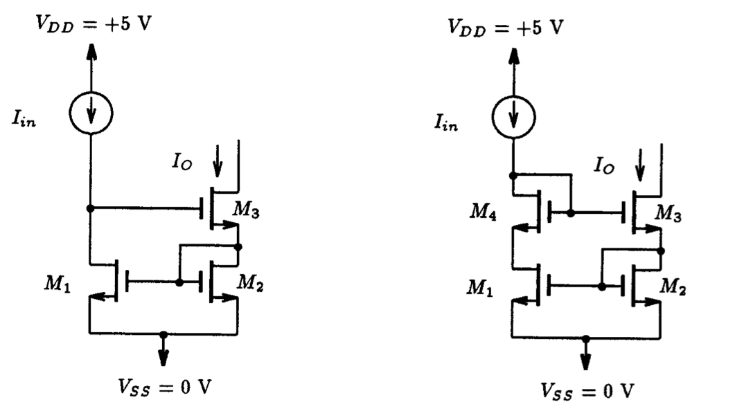
(a) (b)
Fig. P6.11
6.11. In Fig. P6.11(a) we present a NMOS version of the Wilson current mirror. In (b), an additional transistor has been added to the Wilson circuit to make it more symmetrical. Assuming that the MOS devices have Spice model parameters Vt=1 V, 𝜇nCOX=200 𝜇A/V2 and VA=10 V, compare the input-output current behavior of these two mirror circuits.
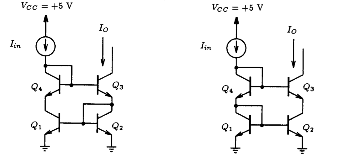
(a) (b)
Fig. P6.12
6.12. Compare the input -- output current behavior (i.e., accuracy, output resistance, minimum output voltage and input current range) of the modified Wilson current mirror circuit shown in Fig. P6.12(a) with the behavior of the cascode current mirror shown in Fig. P6.12(b). Model each bipolar transistor after the Gennum Corporation integrated npn transistor described in section 6.4. Which is the better current mirror? How do these two current mirrors compare with the high-swing cascode-current mirror circuit shown in Fig. 6.18.
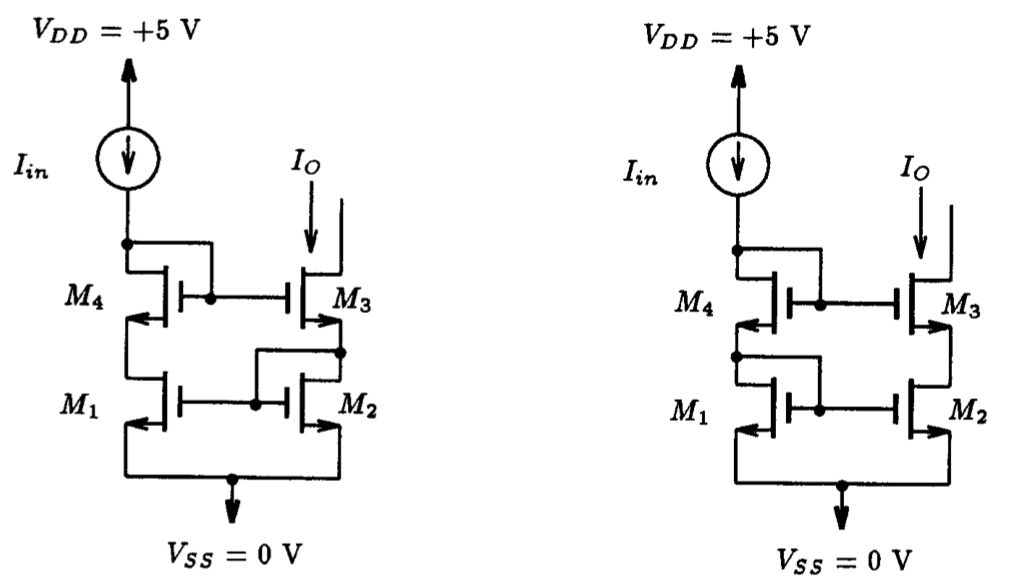
(a) (b)
Fig. P6.13
6.13. Compare the input-output current behavior (i.e., accuracy, output resistance, minimum output voltage and input current range) of the modified Wilson current mirror circuit shown in Fig. P6.13(a) with the behavior of the cascode current mirror shown in Fig. P6.13(b). Assume that the MOS devices have Spice parameters: Vt=1 V, 𝜇nCOX=200 𝜇A/V2 and VA=70 V. Which is the better current mirror? Why are your conclusion here different than that found above in Problem 6.12 for the bipolar case?
6.14. For the high-swing cascode-current mirror shown in Fig. 6.18}, determine the maximum and minimum voltage limits of VB that maintain the current mirror in its linear region. Assume that the transistors are modeled after the integrated npn transistors first suggested in Section 6.4.
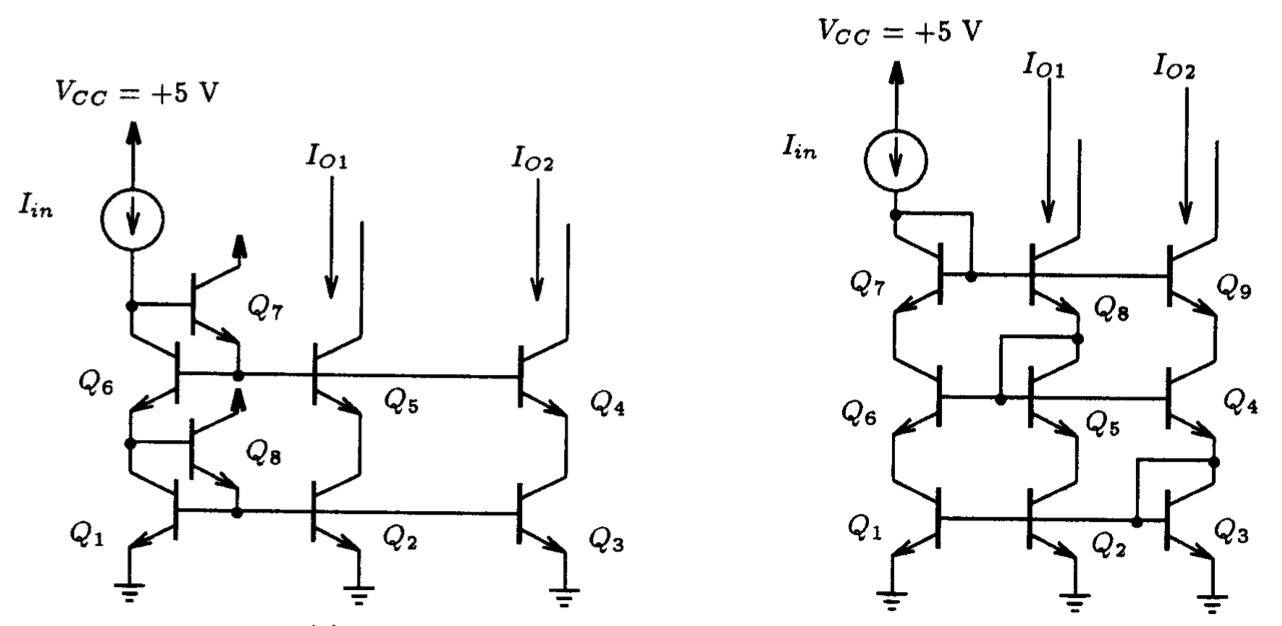
(a) (b)
Fig. P6.15
6.15. In Fig. P6.15 we present two different ways of realizing a two-output current mirror circuit. The circuit in part (a) is a simple extension of the two transistor cascode current mirror circuit. The circuit in part (b) is a generalization of the Wilson current mirror circuit. Assuming that the transistors are modeled after the integrated npn transistor first suggested in Section 6.4, determine using LTSpice which is the better current mirror. Base your judgment on current transfer function accuracy, output resistance, minimum output voltage and input current range.
6.16. Compare your results found in Problem 6.15, with a multiple-output current mirror circuit created by extension of the high-swing cascode-current mirror circuit of Fig. 6.18. Which makes the better multiple-output current mirror?
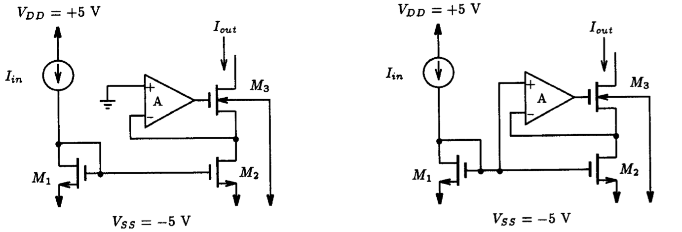
(a) (b)
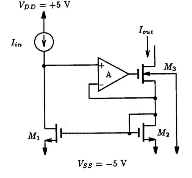
(c)
Fig. P6.17
6.17. To improve the quality of a current mirror, an op-amp of gain A is sometimes used. In Fig. P6.17 we present several possible designs of a MOS current mirror circuit that incorporate an op-amp. For each design, determine using LTSpice how the op-amp gain affects the quality of the current mirror, i.e., (i) current gain accuracy, (ii) output resistance, (iii) minimum output voltage and (iv) input current range. Of the three circuits shown in Fig. P6.17, which behaves closer to the ideal current mirror? Assume the following parameter values for each MOSFET: W=100 𝜇m, L=10 𝜇m, 𝜇nCOX=20 𝜇A/V2, |Vt0|=1 V and 𝜆=0.04 V-1, and 𝛾=0.9 V1/2.
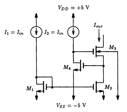
Fig. P6.18
6.18. In Fig. P6.18 we present a high-performance current mirror that is referred to in the literature as a regulated-cascode current mirror. It is assumed that the two input current signals track one another. For an input current level of 1 uA, 10 uA, and 100 uA, determine (a) the current gain accuracy, (b) the output resistance, and (c) the minimum output voltage. Assume the following parameter values for each MOSFET: W=100 𝜇m, L=10 𝜇m, 𝜇nCOX=20 𝜇A/V2, |Vt0|=1 V, 𝜆=0.04 V-1, and 𝛾=0.9 V1/2.
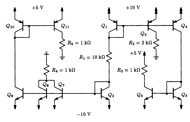
Fig. P6.19
6.19. Compute the voltages at all nodes and the currents through all branches in the circuit of Fig. P6.19 assuming beta is very large using LTSpice. Compare this to the case when B=100.
6.20. Compute the voltages at all nodes and the currents through all branches in the circuit of Fig. P6.19 assuming VA is very large using LTSpice. (Setting VA=0 in the model statement for the BJT is equivalent to setting VA=¥). Compare this to the case when |VA|=100 V.
6.21. Consider the effect of power-supply variation on the dc bias of the op-amp circuit of Fig. 6.36: If +15 V is lowered to +14 V, what is the effect on the amplifier parameters listed in Table 6.6? If, separately, -15 V is raised to -14 V, what is effect on the amplifier parameters in Table 6.6?

Fig. P6.22
6.22. The differential amplifier in Fig. P6.22 is operated with I=100 𝜇A, with devices for which VA=200 V and β=100. What is the differential input resistance, output resistance, equivalent transconductance, and open-circuit voltage gain of this amplifier?
6.23. In the multistage amplifier of Fig 6.36, 100Ω resistors are introduced into the emitter lead of each transistor in the differential pair of the first stage (Q1 and Q2) and 25 Ω for each of the second-stage transistors (Q4 and Q5). With the aid of LTSpice, find the effect that these additions have on the input resistance, the voltage gain of the first stage, and the overall voltage gain.
6.24. If, in the multistage amplifier of Fig. 6.36, the resistor R5 is replaced by a constant-current source of the same value that flows through R5 (i.e., maintain the same bias situation), calculate the overall voltage gain of this amplifier using LTSpice.
6.25. A differential amplifier, utilizing JFETs for which IDSS=2 mA, |VP|=2 V, and VA=100 V, is biased at a constant current of 2 mA. For drain resistors of 10 kΩ, what is the gain of the amplifier for differential output? If the drain resistors have ±1% tolerance, what is the worst-case common-mode gain and CMRR?
Fig. P6.26
6.26. The JFET circuit shown in Fig. P6.26 can be used to implement the current-source bias in a differential amplifier. With the aid of LTSpice, determine the output resistance if IDSS=2 mA, VP=-2 V, and VA=100 V.
6.27. A JFET differential amplifier is loaded with the basic BJT current mirror. The JFETs have VP=-2 V, IDSS=4 mA, and VA=100 V. The BJTs have |VA|=100 V and beta is large. The bias current I=2 mA. Find Ri, Gm, Ro, and the open-circuit voltage gain.
6.28. An NMOS differential pair is to be used in an amplifier whose drain resistors are 100 kΩ ±1%. For the pair, 𝜇nCOX=200 𝜇A/V2 and Vt=1 V. If the output is taken differentially, contrast the voltage gain and input offset voltage of this amplifier for a bias current of 100 𝜇A and 200 𝜇A.
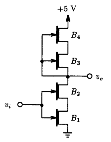
Fig. P6.29
6.29. For the amplifier circuit in Fig. P6.29 let W1=100 𝜇m, W2=500 𝜇m, W3=50 𝜇m, and W4=250 𝜇m. With the aid of LTSpice, compute the voltage gain of this circuit. Assume that the MESFETs are modeled with parameters: Vt=-1 V, B=0.1 mA/V2, and 𝜆=0.1 V-1. Assume that the length of each device is 1 𝜇m.